Method of forming a tantalum-containing layer from a metalorganic precursor

a metalorganic precursor and forming method technology, applied in the field of semiconductor processing, can solve the problems of affecting the quality limiting the utility of the deposited layer in ta film depositing, current ald process, etc., and achieve the effect of improving thermal stability

Inactive Publication Date: 2007-03-08
TOKYO ELECTRON LTD
View PDF8 Cites 47 Cited by
  • Summary
  • Abstract
  • Description
  • Claims
  • Application Information

AI Technical Summary

Benefits of technology

[0011] Embodiments of the invention are directed to addressing any of the above-described and / or other problems with deposition of Ta-containing layers. According to one embodiment of the invention, a non-halogen-containing and non-nitrogen-containing tantalum precursor is utilized to deposit a Ta-containing layer. The Ta-containing layer can be integrated into semiconductor processing as a barrier layer in Cu metallization schemes. The Ta-containing layer may contain tantalum metal, or tantalum carbide, or a combination thereof, and may be deposited by a process such as TCVD, ALD, or PEALD. After deposition, the Ta-containing layer can be processed so as to include tantalum nitride or tantalum carbonitride. The tantalum precursor can contain Ta, a H ligand and a CO ligand. The CO ligand provides the tantalum precursor with improved thermal stability. The tantalum precursor can have the formula (CpR1)(CpR2)TaH(CO), where Cp is a cyclopentadienyl functional group and R1 and R2 are H or alkyl groups.

Problems solved by technology

In addition, plasma excitation may activate layer-forming chemical reactions that are not energetically or kinetically favored in thermal CVD.
However, current ALD processes often suffer from contamination problems that affect the quality of the deposited layers, and thus the manufactured device.
However, the vapor pressures of these precursors are typically no more than about 0.1 torr at 100° C., which limits their utility in depositing Ta films.
Moreover, these precursors do not exclude the use of halogens and / or nitrogen.
The present inventors have recognized that the use of halogen-containing precursors commonly results in high halogen levels in the Ta-containing layers that are unacceptable for integration with other layers in an integrated circuit.

Method used


Image

  • Method of forming a tantalum-containing layer from a metalorganic precursor
  • Method of forming a tantalum-containing layer from a metalorganic precursor
  • Method of forming a tantalum-containing layer from a metalorganic precursor

Examples


Embodiment Construction

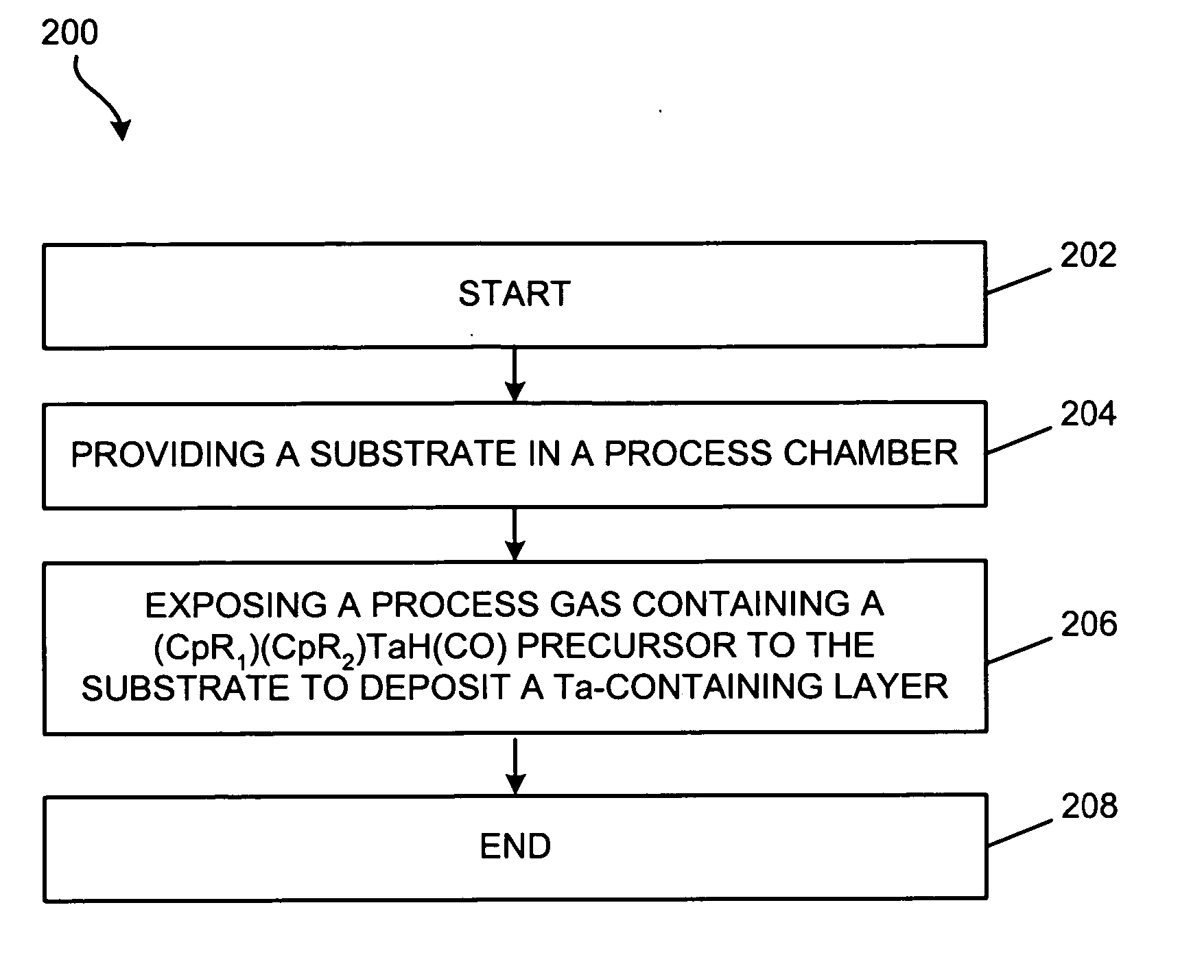
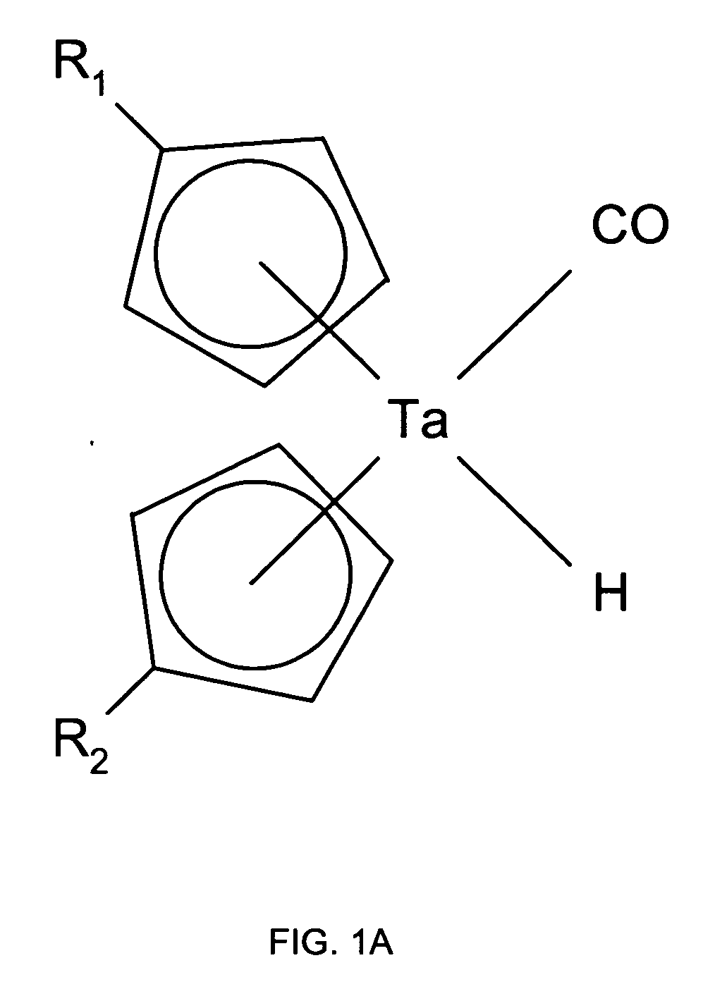
[0026] Embodiments of the invention provide a method and precursor for forming and integrating a Ta-containing layer in semiconductor processing. The tantalum precursor can contain Ta, a H ligand and a CO ligand. The CO improves thermal stability. The CO does not dissociate appreciably during deposition and thus does not significantly oxidize a Ta-containing layer formed from the tantalum precursor or significantly raise the electrical resistivity of the Ta-containing layer. The tantalum precursor can have the formula (CpR1)(CpR2)TaH(CO), where Cp is a cyclopentadienyl functional group and R1 and R2 are H or alkyl groups. FIG. 1A depicts a schematic view of a (CpR1)(CpR2)TaH(CO) precursor.

[0027] An embodiment of the invention includes providing a substrate in a process chamber of a deposition system, exposing a process gas comprising the tantalum precursor to the substrate to form the Ta-containing layer. The Ta-containing layer may be treated to remove contaminants and modify the ...


PUM

PropertyMeasurementUnit
vapor pressureaaaaaaaaaa
temperatureaaaaaaaaaa

Abstract

A method and precursor for forming and integrating a Ta-containing layer in semiconductor processing. The tantalum precursor has the formula (CpR1)(CpR2)TaH(CO), where Cp is a cyclopentadienyl functional group and R1 and R2 are H or alkyl groups. The method includes providing a substrate in a process chamber of a deposition system, and exposing a process gas comprising the tantalum precursor to the substrate to form the Ta-containing layer. The Ta-containing layer may be treated to remove contaminants and modify the layer. The Ta-containing layer may contain tantalum metal, tantalum carbide, tantalum nitride, or tantalum carbonitride, or a combination thereof, and may be deposited in a TCVD, ALD, or PEALD process. A semiconductor device containing a Ta-containing layer formed on a patterned substrate containing one or more vias or trenches is provided.

Description

CROSS REFERENCE TO RELATED APPLICATIONS [0001] The present invention is related to U.S. patent application Ser. No. 11 / 083899, titled “A PLASMA ENHANCED ATOMIC LAYER DEPOSITION SYSTEM AND METHOD”, the entire contents of which are hereby incorporated by reference.FIELD OF THE INVENTION [0002] The present invention relates to semiconductor processing, and more particularly, to a method for forming and integrating a tantalum-containing layer into Cu metallization applications. DESCRIPTION OF RELATED ART [0003] The introduction of copper (Cu) metal into multilayer metallization schemes for manufacturing integrated circuits can necessitate the use of diffusion barriers / liners to promote adhesion and growth of the Cu layers and to prevent diffusion of Cu into the dielectric materials. Barriers / liners that may be deposited onto dielectric materials can include refractive materials, such as tungsten (W), molybdenum (Mo), and tantalum (Ta), that are non-reactive and immiscible in Cu, and can...

Claims


Application Information

Patent Timeline
Patent Type & Authority Applications(United States)
IPC IPC(8): C23C16/00
CPCC23C16/16C23C16/34C23C16/32C23C16/18C23C16/06
Inventor ISHIZAKA, TADAHIROGOMI, ATSUSHI
Owner TOKYO ELECTRON LTD
Why Eureka
Try Eureka