Electrophotographic photoconductor, image forming apparatus, image forming method, and process cartridge

a photoconductor and photoconductor technology, applied in the field of electrostatic photoconductor, image forming apparatus, image forming method, and process cartridge, can solve the problems of image fatal defects, smear and black dots, and dot defects, and achieve small variations in electrostatic characteristics, stable image output, and minimal abnormal images

Inactive Publication Date: 2007-03-15
RICOH KK
View PDF6 Cites 50 Cited by
  • Summary
  • Abstract
  • Description
  • Claims
  • Application Information

AI Technical Summary

Benefits of technology

[0015] An object of the present invention is to provide an electrophotographic photoconductor that generates minimum abnormal images and features small variations in electrostatic characteristics after repetitive use of an image forming apparatus and / or under different usage environments. Another object of the present invention is to provide an image forming apparatus and full-color image forming apparatus that can always achieve stable image output by use of the electrophotographic photoconductor. Still another object of the present invention is to provide a very easy-to-use process cartridge.

Problems solved by technology

The reversal development, however, entails generation of dot defects (e.g., background smear and black dots) at backgrounds (or white solid regions) in a case of charge leakage caused due to minute defects on the photoconductor.
These unwanted dots may be mistaken for dots in a drawing or for periods and / or commas in an English document; therefore, they are fatal defects for images.
In most cases, these defects are mainly attributed to partial charge leakage from the photoconductor.
Major challenges to this problem include improving the pressure resistance of the photoconductor, improving the uniformity of charge distribution over the photoconductor surface, and keeping voltage more constant.
In this case, the intermediate layer is produced through wet coating process and thus it is difficult to avoid generation of pinholes in the film being made.
For this reason, the intermediate layer may not be as effective as expected.
Intermediate layers composed of dispersed filler resin as disclosed in JP-A Nos.58-58556, 60-111255, 59-17557, 60-32054, 64-68762, 64-68763, 64-73352, 64-73353, 1-118848 and 1-118849, however, contain ultrafine filler particles of submicron or smaller sizes, which are too costly and bulky to be used.
Such submicron particles entail re-aggregation of filler particles in their dispersion or upon deposition of film to result in film thickness variations of 1 μm or greater in some cases, making it impossible to provide an intermediate layer that allows designing of a photoconductor with uniform charge distribution and constant voltage.
Under such circumstances, how electrostatic characteristics of the photoconductor can be made constant even after repetitive use and / or under different usage environments is a great challenge to be tackled.
As described above, since image defects such as background smear are caused due primarily to charge leakage, the likelihood of charge leakage is dependent on the electric field intensity; the higher the intensity, the more likely it is that charge leakage occurs.
However, problems specific to the protection layer have occurred.
For example, the amount of substance that accumulates on the surface of the photoconductor after repetitive use increases due to the reduced wear volume of the surface protective layer, resulting in creation of abnormal images (e.g., blurred images).
Thus, a long time usage of photoconductor has been made possible, which seems to be impossible with photoconductor having no surface protective layers.
Electrostatic fatigue has unexpectedly become a life-determining factor of photoconductor in terms of image defects caused due to photoconductor wearing out and charge leakage.

Method used


Image

  • Electrophotographic photoconductor, image forming apparatus, image forming method, and process cartridge
  • Electrophotographic photoconductor, image forming apparatus, image forming method, and process cartridge
  • Electrophotographic photoconductor, image forming apparatus, image forming method, and process cartridge

Examples


synthesis example 1

PIGMENT SYNTHESIS EXAMPLE 1

Synthesis of Titanyl Phthalocyanine Crystal

[0359] A pigment was prepared in accordance with the method disclosed in JP-A No.2001-19871. More specifically, 29.2 g of 1,3-diiminoisoindoline was mixed with 200 ml of sulfolane, and 20.4 g of titanium tetrabutoxide was added dropwise to the mixture under nitrogen flow. Thereafter, the resultant mixture was gradually heated to 180° C., allowing reaction to take place for 5 hours at 170° C. to 180° C. with agitation. After cooled down, the resulting precipitate was recovered by filtration, washed with chloroform until it became blue, washed with methanol for several times, washed with 80° C. hot water for several times, and dried to produce coarse titanyl phthalocyanine particles. The coarse titanyl phthalocyanine particles were dissolved in 20 volumes of concentrated sulfuric acid, and the resulting mixture was added dropwise to 100 volumes of ice water with agitation. The crystals thus precipitated were recov...

synthesis example 2

PIGMENT SYNTHESIS EXAMPLE 2

Synthesis of Titanyl Phthalocyanine Crystal

[0369] An aqueous paste of a titanyl phthalocyanine pigment was prepared in accordance with the method described in Pigment Synthesis Example 1, and subjected to crystal conversion in the manner described below to produce a titanyl phthanylcyanine crystal having primary particles smaller than those of the titanyl phthanylcyanine crystal prepared in Pigment Synthesis Example 1.

[0370] In accordance with Example 1 of JP-A No.2004-83859, 400 parts of tetrahydrofuran was added to 60 parts of the aqueous paste prepared in Pigment Synthesis Example 1, an aqueous paste of titanyl phthanylcyanine prior to crystal conversion, and vigorously stirred using a homomixer (MARKIIf, KENIS, Ltd.) at 2,000 rpm at room temperature until the color of the paste changed from navy blue to light blue (about 20 minutes after initiation of stirring), followed by immediate filtration under vacuum. The crystals on the filtration device wer...

example 1-1

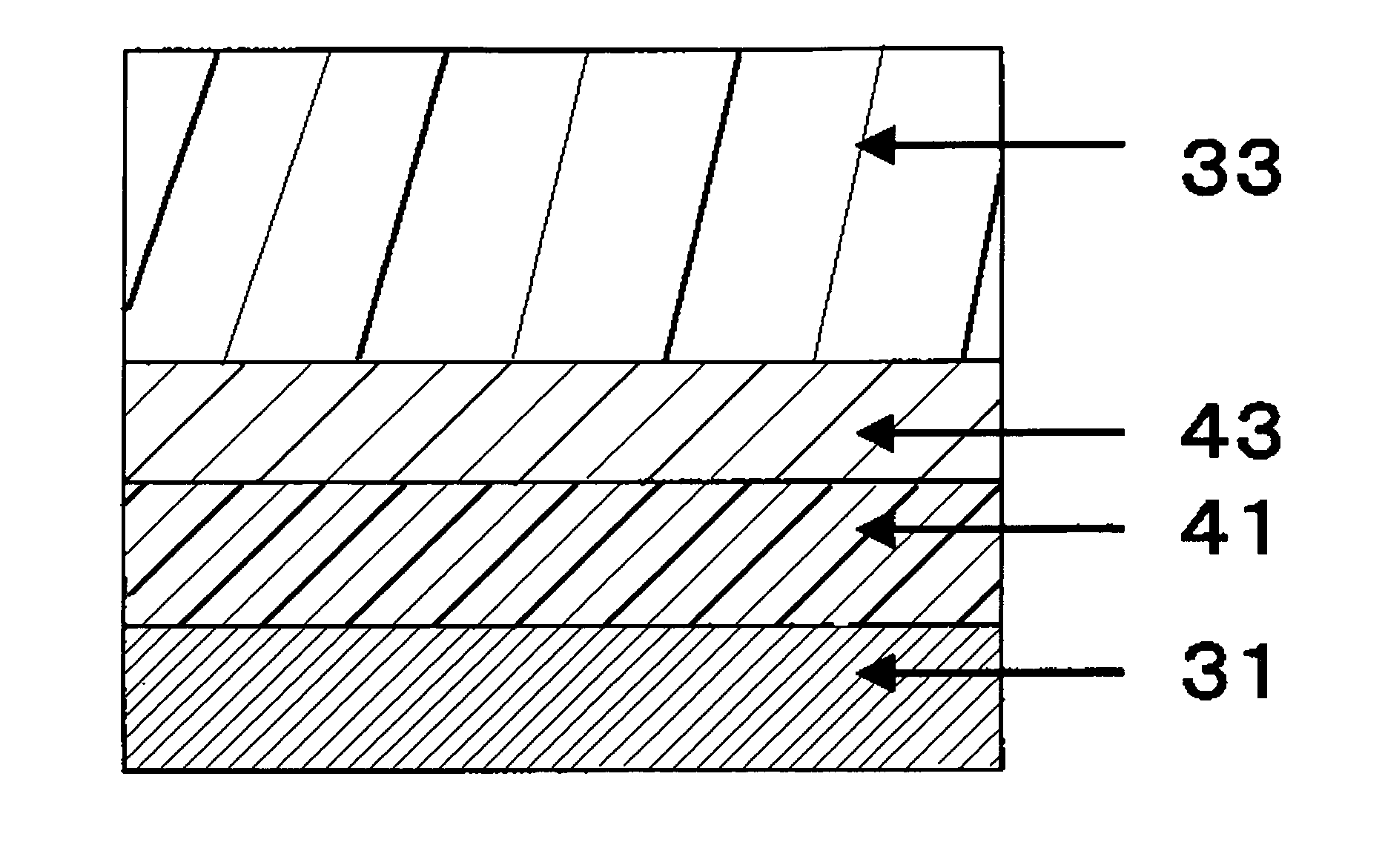
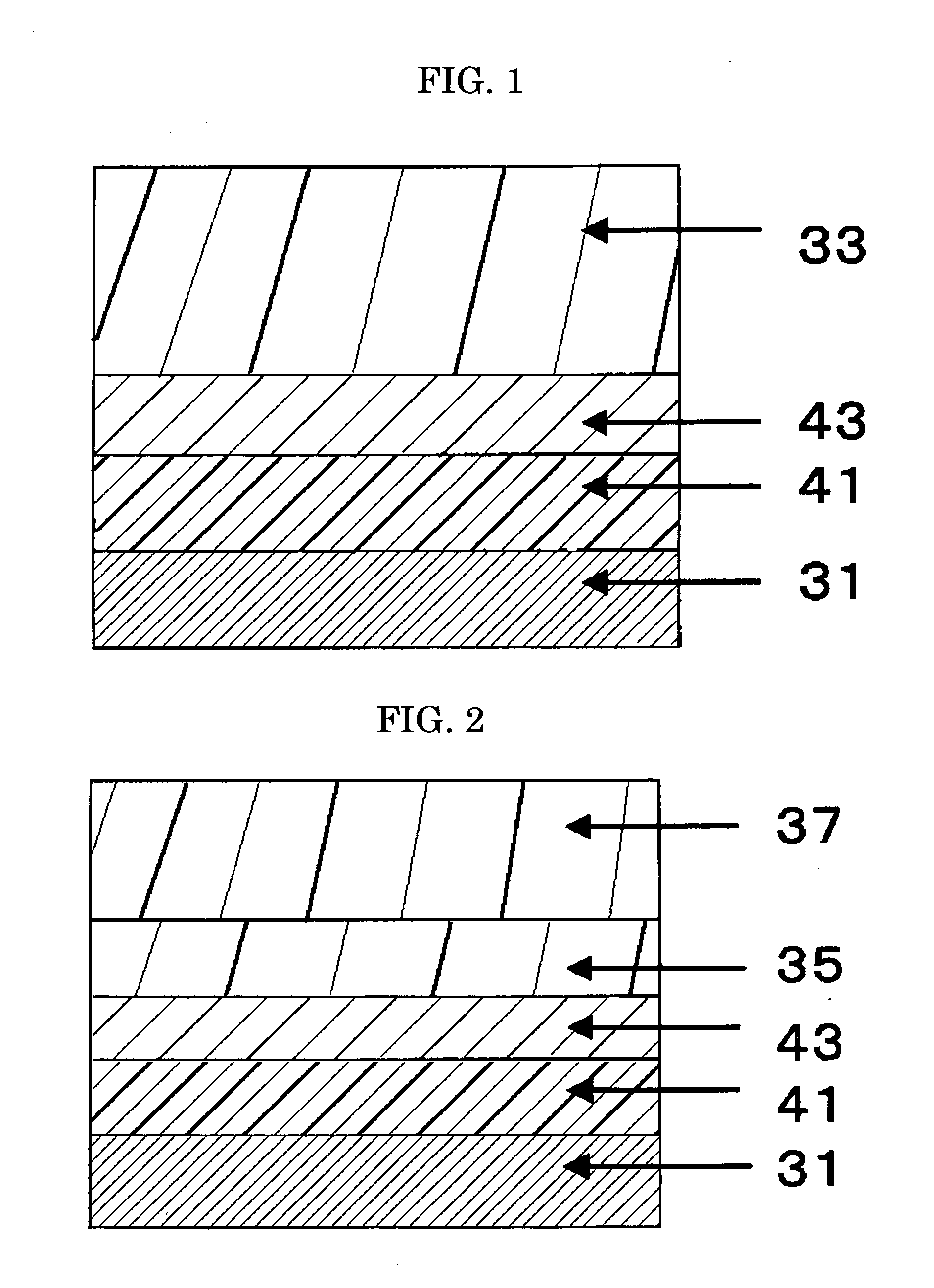
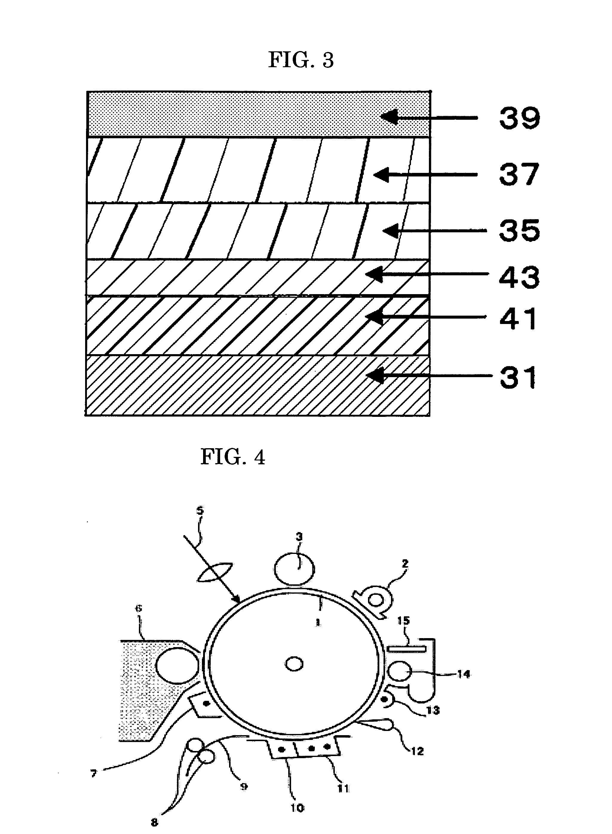
[0376] An aluminum cylinder of 340 mm length and 30 mm diameter (JIS1050) was adopted as a conductive support, and the following coating solution for charge blocking layer, coating solution for moire preventing layer, coating solution for charge generating layer, and coating solution for charge transporting layer were sequentially applied on the conductive support and dried to produce a photoconductor provided with a charge blocking layer of 0.5 μm thickness, a moire preventing layer of 3.5 μm thickness, a charge generating layer of 0.3 μm thickness, and a charge transporting layer of 25 μm thickness (hereinafter referred to as “Photoconductor 1”).

N-methoxymethylated nylon (FR101, Namariichi Co., Ltd.) 5 PartsMethanol70 Partsn-Butanol30 Parts

[0377]

Titanium oxide (CR-EL, Ishihara Sangyo Kaisha, Ltd.  84 PartsAverage particle diameter = 0.25 μm)Alkyd resin (BEKKOLITE M6401-50-S, Dainippon Ink &33.6 PartsChemicals, Inc., solid content = 50%)Melamine resin (SUPER BEKKAMIN L-121-60,18....


PUM


Abstract

To provide an electrophotographic photoconductor that has a layer containing a compound represented by the following general formula (1), and an image forming apparatus using the electrophotographic photoconductor.
    • where R1 and R2 independently represent any one of a hydrogen atom, substituted or unsubstituted alkyl group, substituted or unsubstituted cycloalkyl group and substituted or unsubstituted aralkyl group, and R3, R4, R5, R6, R7, R8, R9 and R10 independently represent any one of a hydrogen atom, halogen atom, cyano group, nitro group, amino group, hydroxyl group, substituted or unsubstituted alkyl group, substituted or unsubstituted cycloalkyl group and substituted or unsubstituted aralkyl group

Description

BACKGROUND OF THE INVENTION [0001] 1. Field of the Invention [0002] The present invention relates to an image forming apparatus that involves an electrostatic copying process for image forming (e.g., a copier, facsimile machine, and printer), a process cartridge provided to the image forming apparatus, and an image forming method adopted for the image forming apparatus. [0003] 2. Description of the Related Art [0004] In recent years, information processing systems that utilize electrophotography have been remarkably developed. In particular, photoprinters that covert information into digital signals for information recording by means of light beam have been remarkably successful in terms of their print quality and reliability. This digital recording technology is applied not only to printers, but also to general copiers, and therefore, the development of so-called digital copiers has been made. In addition, since analogue copiers that utilize this digital recording technology are pr...

Claims


Application Information

Patent Timeline
Patent Type & Authority Applications(United States)
IPC IPC(8): G03G5/14G03G5/147
CPCG03G5/0614G03G5/0651G03G5/0696G03G5/071G03G5/14791G03G5/14704G03G5/14734G03G5/14786G03G5/144G03G5/072G03G5/0745G03G5/0732G03G5/074
Inventor SHIMOYAMA, KEISUKEKURIMOTO, EIJIORITO, TAKESHINIIMI, TATSUYAKAWAMURA, SHINICHIYANAGAWA, YOSHIKISASAKI, MICHITAKA
Owner RICOH KK
Why Eureka
Try Eureka