
Semiconductor device

a technology of semiconductor devices and nodes, applied in the direction of semiconductor devices, electrical equipment, transistors, etc., can solve the problems of reduced operational speed, soft error, and recognized problems, and achieve the effect of suppressing the potential change preventing the inversion of the logic type of the drain region, and increasing the capacitance of the nod

Active Publication Date: 2007-03-22
RENESAS ELECTRONICS CORP
View PDF6 Cites 20 Cited by
  • Summary
  • Abstract
  • Description
  • Claims
  • Application Information

AI Technical Summary

Benefits of technology

[0021] According to the semiconductor device of the present invention, since the drain regions are formed away from each other, even if radiation is applied to one drain region, and holes or electrons (collectively referred to as “charges”) are generated, an amount of collected charges relative to the total drain area is smaller than that of a field effect transistor having only one drain region. Thus, it is possible to prevent inversion of a logic type of a drain region.
[0022] Further, since the drain region is enlarged to increase a node capacitance, even if charges are generated due to the radiation, a potential change of the drain region can be suppressed.
[0023] Further, the drain regions are formed on opposite sides of the source region, so charges rarely gather into each drain region at the same time. This is because, even if charges are generated in one drain region, the charges are mostly absorbed by the source region interposed between the drain regions, and an amount of charges that reach the other drain region can be reduced. Accordingly, a logic type of the drain region is hardly inverted, so an SET resistance can be increased.
[0024] Furthermore, drain regions are formed away from each other, and a common source region is provided for the drain regions, whereby a layout area of the source region can be reduced, making it possible to minimize the total layout area.

Problems solved by technology

Along with recent miniaturization in a semiconductor process of a semiconductor device composed of field effect transistors such as MOSFETs, a transient error (soft error) resulting from radiation (for example, high-energy neutron radiation, thermal neutron radiation, and a radiation) has been recognized as a problem.
The SEU causes a problem of, for example, data inversion that data stored in a memory cell is different from the original data.
However, if this countermeasure is adopted against a SEU that occurs in a circuit transmitting a clock signal or the like, an operational speed is reduced or a chip area is considerably increased, so this countermeasure is inappropriate.
However, incorporating the majority circuit or coincidence circuit increases a circuit area, so there is a possibility that necessary functional parts cannot be embedded in a limited area.
The clock phase shift leads to a problem in that a synchronizing circuit using the clock causes a malfunction.
Thus, there is a problem in that this circuit cannot be applied to a circuit that operates all the time like the ring oscillator circuit.

Method used


Image

  • Semiconductor device
  • Semiconductor device
  • Semiconductor device

Examples


first embodiment

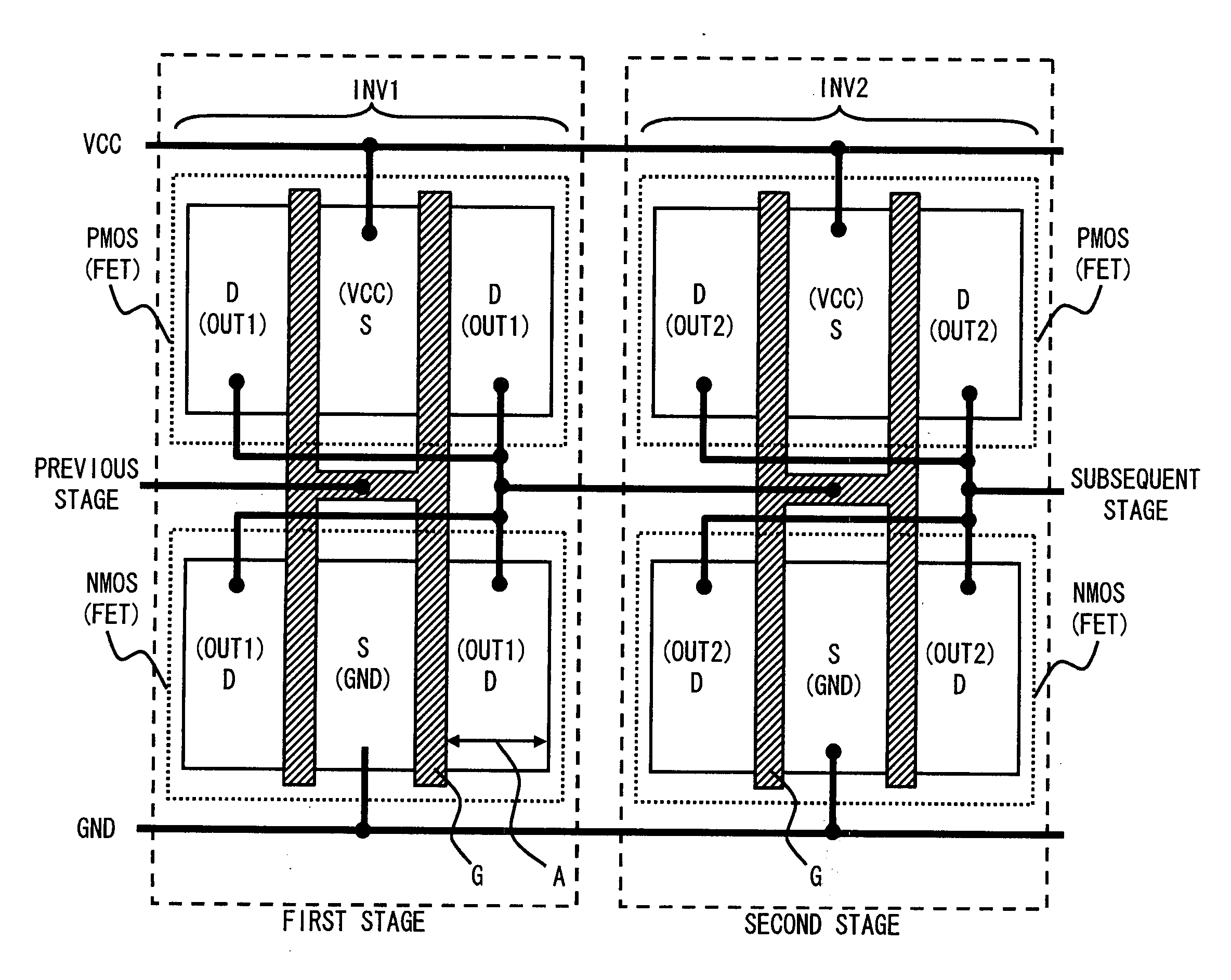
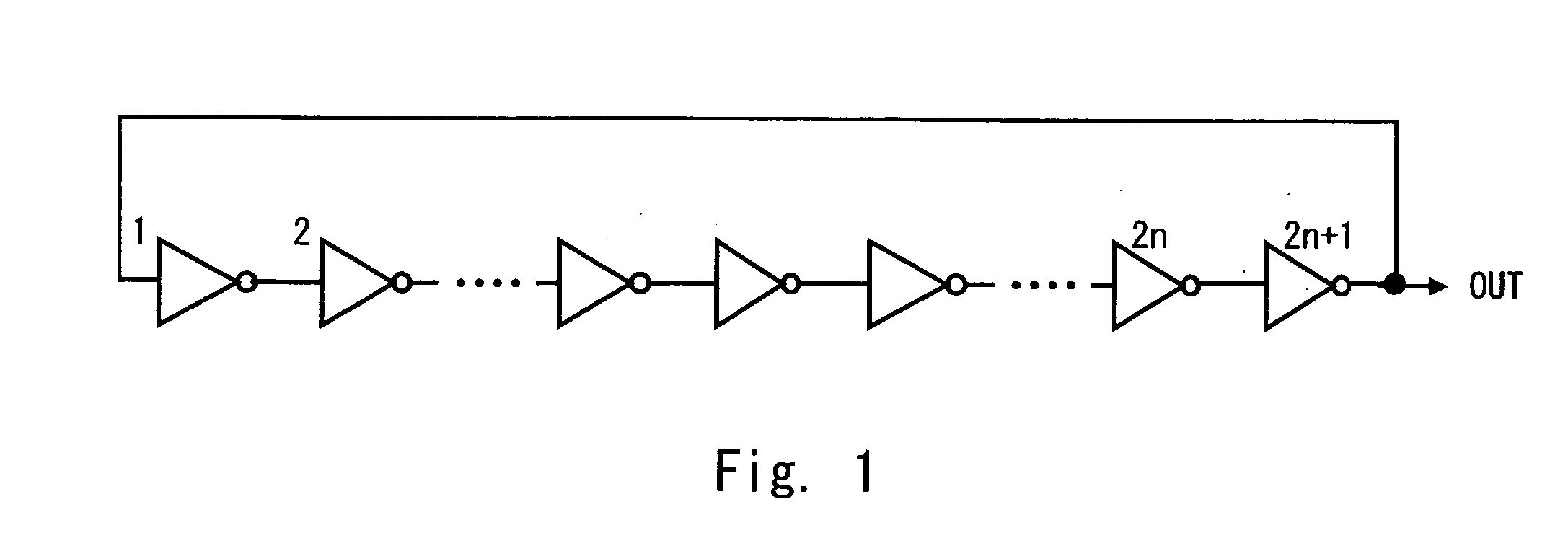
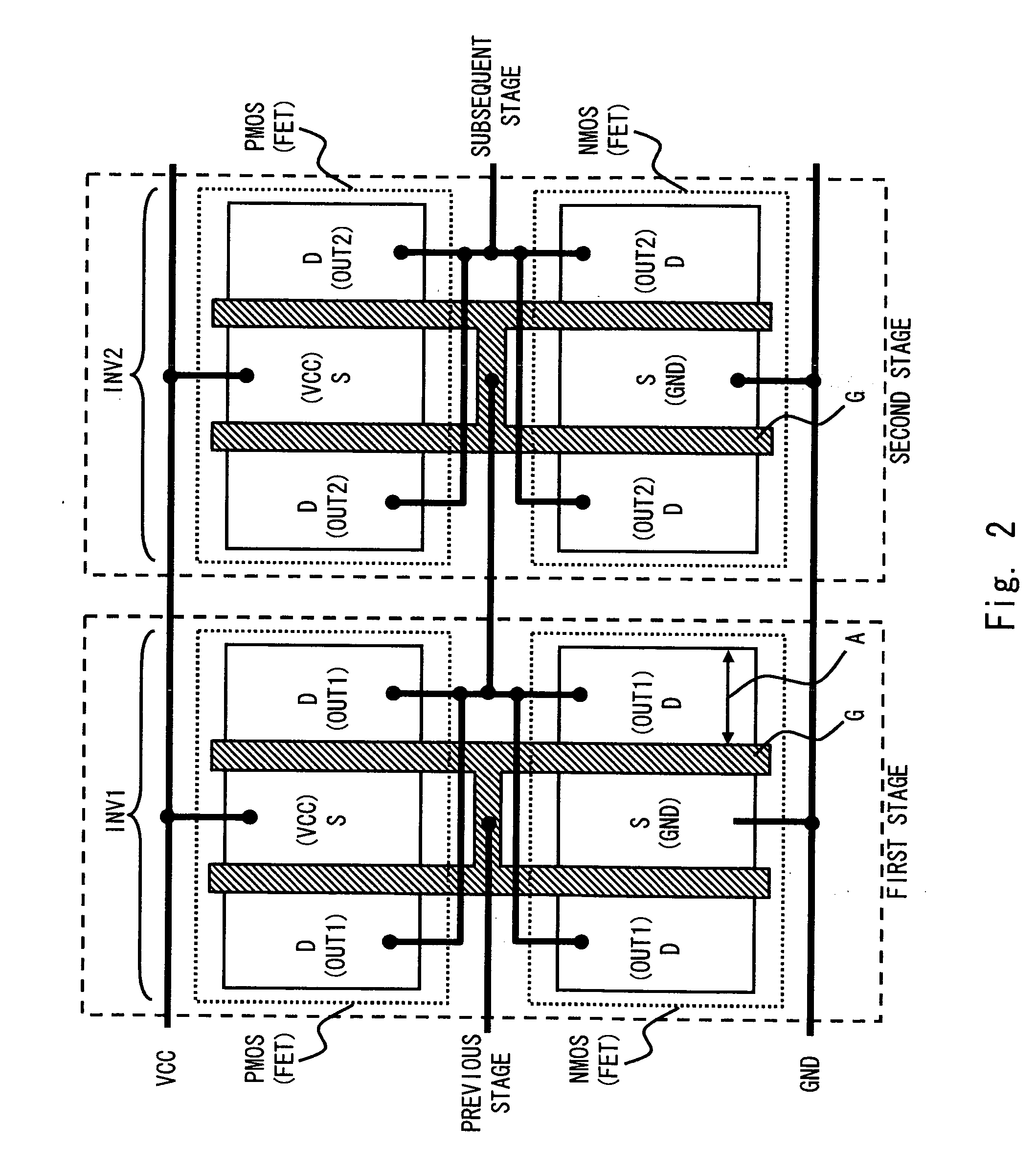
[0038]FIG. 1 shows an oscillating circuit according to a first embodiment of the present invention (for example, ring oscillator circuit). As shown in FIG. 1, the ring oscillator circuit is composed of an odd number of logic circuits (for example, inverter circuit) which are connected in series. The ring oscillator circuit of this embodiment is formed on, for example, a silicon semiconductor substrate. FIG. 2 shows a layout of two of inverter circuits that constitute the ring oscillator circuit.

[0039] Referring to FIG. 2, the layout of the first embodiment is described in detail. As shown in FIG. 2, each inverter circuit has two field effect transistors (for example, PMOS transistor and NMOS transistor). The inverter circuits are connected in series so as to function as the ring oscillator circuit. In the following description, the direction from the left to the right of FIG. 2 is referred to as the X direction, and the upward direction of FIG. 2 is referred to as the Y direction. ...

second embodiment

[0051]FIG. 3 shows a layout of an inverter circuit according to a second embodiment of the present invention. The layout of the inverter circuit of the second embodiment differs from that of the inverter circuit of the first embodiment in that a well potential diffusion layer region well (N-type diffusion layer) and a substrate potential diffusion layer region sub (P-type diffusion layer) are added between the two inverter circuits. The same layout portion as that of the first embodiment is assigned with identical reference numerals and description thereof is omitted here.

[0052] The layout of the inverter circuit of the second embodiment is described as below. The inverter circuit of the second embodiment has the well potential diffusion layer region well and the substrate potential diffusion layer region sub provided between two adjacent inverter circuits. The well potential diffusion layer region well is connected with the power supply potential VCC, and is formed between two adj...

third embodiment

[0055]FIG. 4 shows a layout of an inverter circuit according to a third embodiment of the present invention. A layout of the inverter circuit of the third embodiment differs from that of the inverter circuit of the second embodiment in that the numbers of source regions and drain regions of each transistor are increased. The same layout portion as that of the second embodiment is denoted by identical reference numerals, and description thereof is omitted here.

[0056] The layout of the inverter circuit of the third embodiment is described in detail below. The layout of the inverter circuit of the third embodiment is substantially the same as that of the inverter circuit of the first embodiment. The following description is focused on a difference between the first embodiment and the third embodiment.

[0057] The gate electrode G of this embodiment extends in the Y direction with a rectangular shape. Four gate electrodes G are provided for each transistor pair (the NMOS transistor and ...


PUM


Abstract

A semiconductor device according to an embodiment of the invention includes: a plurality of field effect transistors; and a plurality of logic circuits composed of the field effect transistors, the field effect transistors each including: first and second drain regions formed away from each other; at least one source region formed between the first and second drain regions; and a plurality of gate electrodes formed between the first drain region and the source region and between the second drain region and the source region.

Description

BACKGROUND OF THE INVENTION [0001] 1. Field of the Invention [0002] The present invention relates to a semiconductor device, and more particularly to a semiconductor device layout effective for suppressing soft errors. [0003] 2. Description of Related Art [0004] Along with recent miniaturization in a semiconductor process of a semiconductor device composed of field effect transistors such as MOSFETs, a transient error (soft error) resulting from radiation (for example, high-energy neutron radiation, thermal neutron radiation, and a radiation) has been recognized as a problem. As an example of the soft error, there is SEU (Single Event Upset) that logic inversion occurs due to charges accumulated in a node decrease due to charges resulting from radiation. In general, the occurrence of the SEU depends on a trade-off between an amount of charges accumulated in an information storage node (node voltage * node capacitance) and an amount of charges gathered to the information storage node...

Claims


Application Information

Patent Timeline
Patent Type & Authority Applications(United States)
IPC IPC(8): H01L29/94
CPCH01L27/0207H01L27/1104H01L27/092H10B10/12
Inventor FURUTA, HIROSHITAKAHASHI, HIROYUKI
Owner RENESAS ELECTRONICS CORP
Learn More