[0013] The following presents a simplified summary in order to provide a basic understanding of one or more aspects of the invention. This summary is not an extensive overview of the invention, and is neither intended to identify key or critical elements of the invention, nor to delineate the scope thereof. Rather, the primary purpose of the summary is to present some concepts of the invention in a simplified form as a prelude to the more detailed description that is presented later. The invention relates to an array structure of single-level poly EEPROM memory cells (e.g., NMOS memory cells) and method of operating the array. The EEPROM array is implemented in a higher density embedded EEPROM
layout that eliminates the use of
high voltage transistors from the array core region. If the
high voltage transistors are utilized, they are moved to row and column drivers in the periphery region to increase array density in the core region with little or no added
process complexity. This arrangement permits economic implementation of larger embedded SLP EEPROM arrays that have minimal process complexity. During program or erase operations of the array, the method provides a
programming voltage comprising first and second half-write voltages associated with the row and column driver circuits, respectively, that are applied to the selected memory cells of the array, and one of the first and second half-write (e.g., mid-level, half-
programming) voltages or less applied to the remaining unselected memory cells. Beneficially, this half-write method of operation further enables the operation of a lower voltage driver
transistor, does not enable writing to the unselected memory cells, and avoids disturbing the unselected memory cells of the array.
[0015] The half-write scheme of the present invention relies on the principle that the magnitude of the F-N
tunneling current at the half-write voltage (e.g., about half the programming voltage) is small enough that non-selected bits are not written into or otherwise disturbed. The half-write scheme of the present invention is compatible with most existing SLP EEPROM
schematic cell designs. The number of lead wires or interconnections per row and per column will vary depending on the
cell design selected. The half-write scheme puts less voltage stress on some circuit nodes and allows the use of new smaller SLP EEPROM bits. The methods and structure described herein are applicable to
silicon wafer fabrication and other such fabrication processes in the manufacture of
semiconductor memory devices.
[0017] For example, the half-write method of the present invention enables the transistors of the core to be fabricated from
low voltage devices (e.g., 3.3
volt transistors) that operate for a short period of time at nearly double that voltage (e.g., about 6 volts, a half-write voltage level). Then, by combining the half-write voltage applied to a row (e.g., about +6 volts), with another (complementary) half-write voltage applied to a column of cells (e.g., about −6 volts), a higher differential voltage (e.g., about 12 volts) is obtained across a selected
cell, or group of cells, suitable to program or erase the selected
memory cell(s).
[0018] A cell is programmed, for example, by applying one polarity voltage to the cell (e.g., about +12 volts), while the cell is erased by applying the opposite polarity programming voltage to the cell (e.g., about −12 volts). Similarly, the innovative method of the present invention further enables the row and column driver circuits to be fabricated using conventional lower voltage
CMOS transistors in the level-shifter circuits, which traditionally use
high voltage transistors. This is because these circuits now only need to withstand the half-write voltage levels (e.g., about 6 volts) for then only for a short period of time. Further, any number of cells of the array may be programmed or erased in this manner by selecting and applying programming voltage levels to any number of rows and columns associated with the selected cells, which will apply no more than about the half-write voltage or less (down to and including no voltage) to the unselected cells.
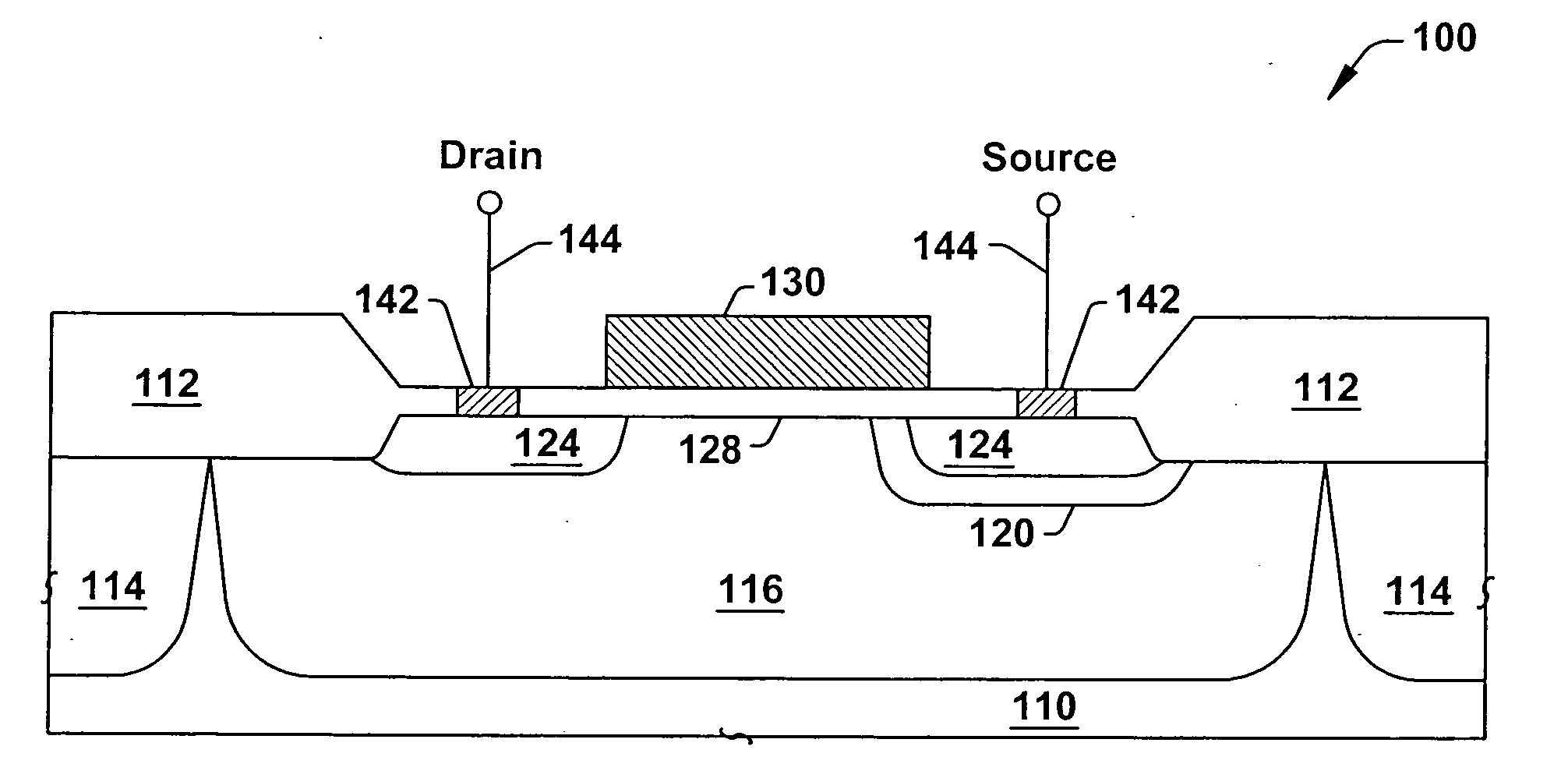
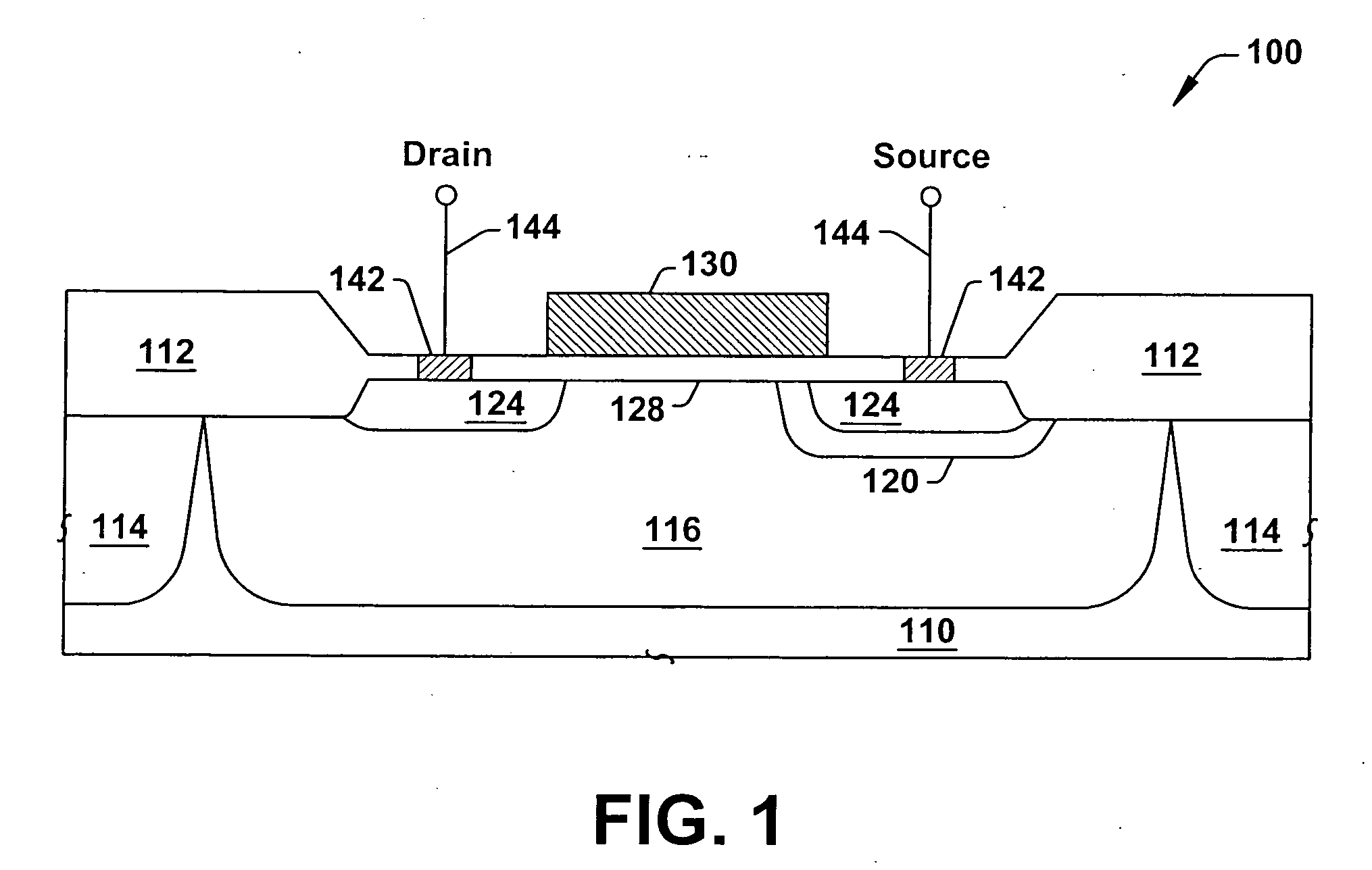
[0030] In still another aspect of the invention, the semiconductor process may use a
dielectric isolated technology for SLP EEPROM where no junction in the array sees more than the half-write voltage, to further simplify structures and reduce the
wafer area.

