Method and apparatus for CMOS imagers and spectroscopy

a spectroscopic and optical imaging technology, applied in the field of spectroscopy, can solve the problems of reducing the minimum size of such optical analysis systems, limiting the spectral resolution of grating-based spectrometer geometries, and many semiconductor-based microfluidic structures previously proposed, and unable to perform optical analysis of device contents in the visible and near-uv spectral ranges

Inactive Publication Date: 2007-03-29
CALIFORNIA INST OF TECH
View PDF4 Cites 91 Cited by
  • Summary
  • Abstract
  • Description
  • Claims
  • Application Information

AI Technical Summary

Benefits of technology

[0017] Also, although the illustrated embodiment uses no lenses between the imaging array and the fluidic channels, it is sometimes of advantage to introduce an imaging lens. Therefore, the use of a compact system t...

Problems solved by technology

However, miniaturization of grating-based spectrometer geometries ultimately is limited by a reduction of the spectral resolution, which can be predicted from the optical path-lengths between the grating and the detection slit.
This compromise between resolution, insertion losses and size has in the past limited the minimum size of such optical analysis systems.
Many semiconductor based microfluidic structures previously proposed have suffered from the inability to perform optical analy...

Method used


Image

  • Method and apparatus for CMOS imagers and spectroscopy
  • Method and apparatus for CMOS imagers and spectroscopy
  • Method and apparatus for CMOS imagers and spectroscopy

Examples


Embodiment Construction

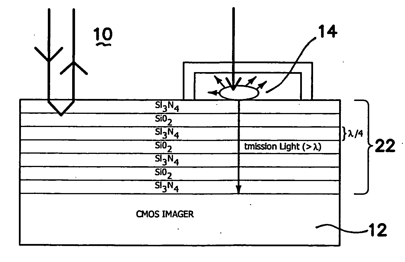
[0052] CMOS Absorption Spectroscopy

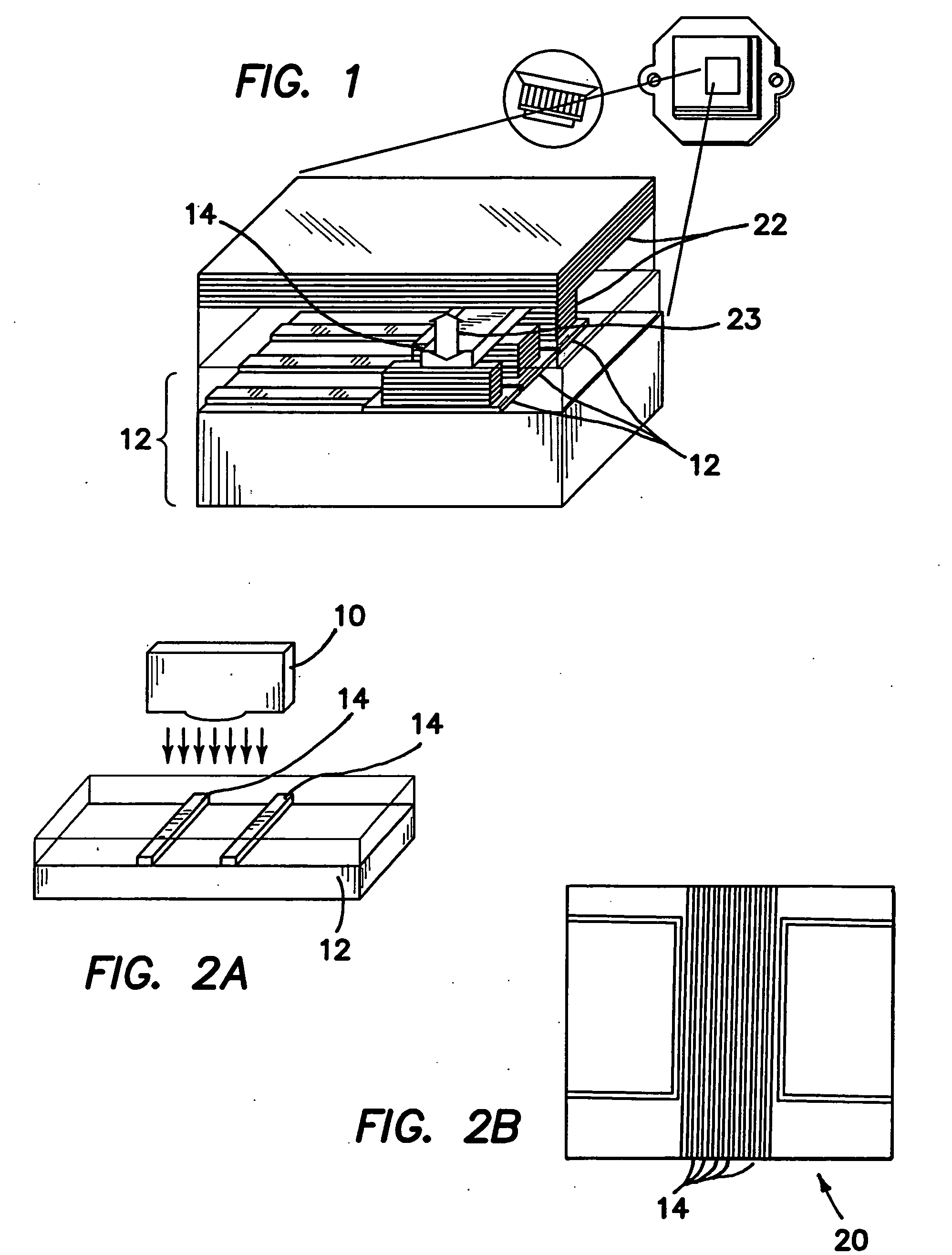
[0053] Consider first the general concept of CMOS absorption spectroscopy. The external optical excitation and read-out devices described in the illustrated embodiment include a 588 nm light emitting diode 10 and a CMOS camera chip 12. One key difference between an absorption spectroscopy measurement system and a more conventional cell-sorting system is that no lenses are used for imaging in the absorption spectroscopy measurement system. This simple approach to reducing the size of a spectroscopic imaging system eliminates the need for focusing optics by placing the microfluidic devices 14 directly onto the CMOS camera chip or imaging detector array 12.

[0054] The imaging detector array 12 in one embodiment is comprised of silicon-based avalanche photodiodes (APDs), charge coupled devices (CCDs), or CMOS integrated p-n diode sensors. All of these devices are commercially available at reasonable costs. CCD arrays, although in general more sensitiv...


PUM


Abstract

A miniaturized fluidic spectrometer comprises a light source, a fluidic circuit having a plurality of flow channels through which an analyte flows, and a proximity detector array for detecting light from the light source transmitted through the fluidic circuit. Where the light source is broadband, a variable filter is disposed between the detector array and the fluidic circuit so that each position of the detector array is provided with a different wavelength response. The fluidic circuit is disposed in an optimized Fabry-Perot etalon. The fluidic circuit is defined in an elastomeric material and includes means for tuning the Fabry-Perot etalon by pressurization of flow channels in the elastomeric material.

Description

RELATED APPLICATIONS [0001] The present application is related to U.S. Provisional Patent Application Ser. No. 60 / 688,643, filed Jun. 8, 2005, which is incorporated herein by reference and to which priority is claimed pursuant to 35 USC 119.GOVERNMENT RIGHTS [0002] This invention was funded in part by support from the U.S. Army, contract grant no. DAAD19-00-1-0392. The Government has certain rights.BACKGROUND OF THE INVENTION [0003] 1. Field of the Invention [0004] The invention relates to the field of CMOS imagers and spectroscopy in miniaturized systems. [0005] 2. Description of the Prior Art [0006] Over the past few years, the use of replication molding for the definition of microfluidic systems in elastomers has allowed the rapid development of compact analysis systems used for chemical sensing and biological diagnostics. For example, fluorescently activated cell sorters based on pumps, valves and channels defined in RTV silicone elastomers have demonstrated excellent throughput...

Claims


Application Information

Patent Timeline
IPC IPC(8): G01J3/26G01B9/02
CPCG01J3/02G01J3/0256G01J3/26G01N21/0303G01N21/031G01N2021/0346G01N21/645G01N2021/058G01N2021/6417G01N2021/6482G01N21/05
Inventor SCHERER, AXELADAMS, MARK
Owner CALIFORNIA INST OF TECH
Why Eureka
Try Eureka