High speed on-chip serial link apparatus and method

a serial link, high-speed technology, applied in the direction of digital transmission, generating/distributing signals, instruments, etc., can solve the problems of long manufacturing test cycle, long delay in transfer debug information, slow power-on sequence, etc., to maximize the speed of the serial interface, and maximize the performance

Active Publication Date: 2007-04-05
MICROSOFT TECH LICENSING LLC +1
View PDF5 Cites 14 Cited by
  • Summary
  • Abstract
  • Description
  • Claims
  • Application Information

AI Technical Summary

Benefits of technology

[0012] Another advantage of the present invention is that the conversion from the standard interface to HSSL is only limited by the performance of the external interface components used. A limitation of the serial clock speed as caused by the usage of the first state-of-the-art approach discussed above does not occur. For example, for an approach using a distributed serial clock with a frequency much slower than the system cycle, the frequency ratio with a system clock of 1 Ghz would be at least 1:1000 to satisfy the direct current (DC) physical design rules. The mechanism of the present invention operates at the same clock speed and frequency as the system clock.
[0013] With the mechanism of the present invention, an additional distributed clock-tree is not required, such as would be required in the second state-of-the-art solution discussed above. The present invention avoids the need for an additional distribution clock-tree due to the fact that the system clock is used for the HSSL and the converter is placed near the external interface. Thus, the negative physical design impacts as caused by implementing the second state-of-the-art approach discussed above are avoided.
[0014] The mechanism of the present invention enables the maximum speed for the serial interface, which is crucial in power-on-reset (POR), manufacturing testing, and chip debugging. With POR, many chips require loading of configuration data to initialize registers and memories. As a function of the amount of data, the interface speed has a direct impact on the boot time of a system. The present invention maximizes the speed of

Problems solved by technology

These low clock frequencies result in slow power-on sequences, long manufacturing test cycles per chip, and long delays to transfer debug information during the chip “bring-up” phase.
This replication results in a large overhead with regard to silicon area and an additional clock distributio

Method used


Image

  • High speed on-chip serial link apparatus and method
  • High speed on-chip serial link apparatus and method
  • High speed on-chip serial link apparatus and method

Examples


Embodiment Construction

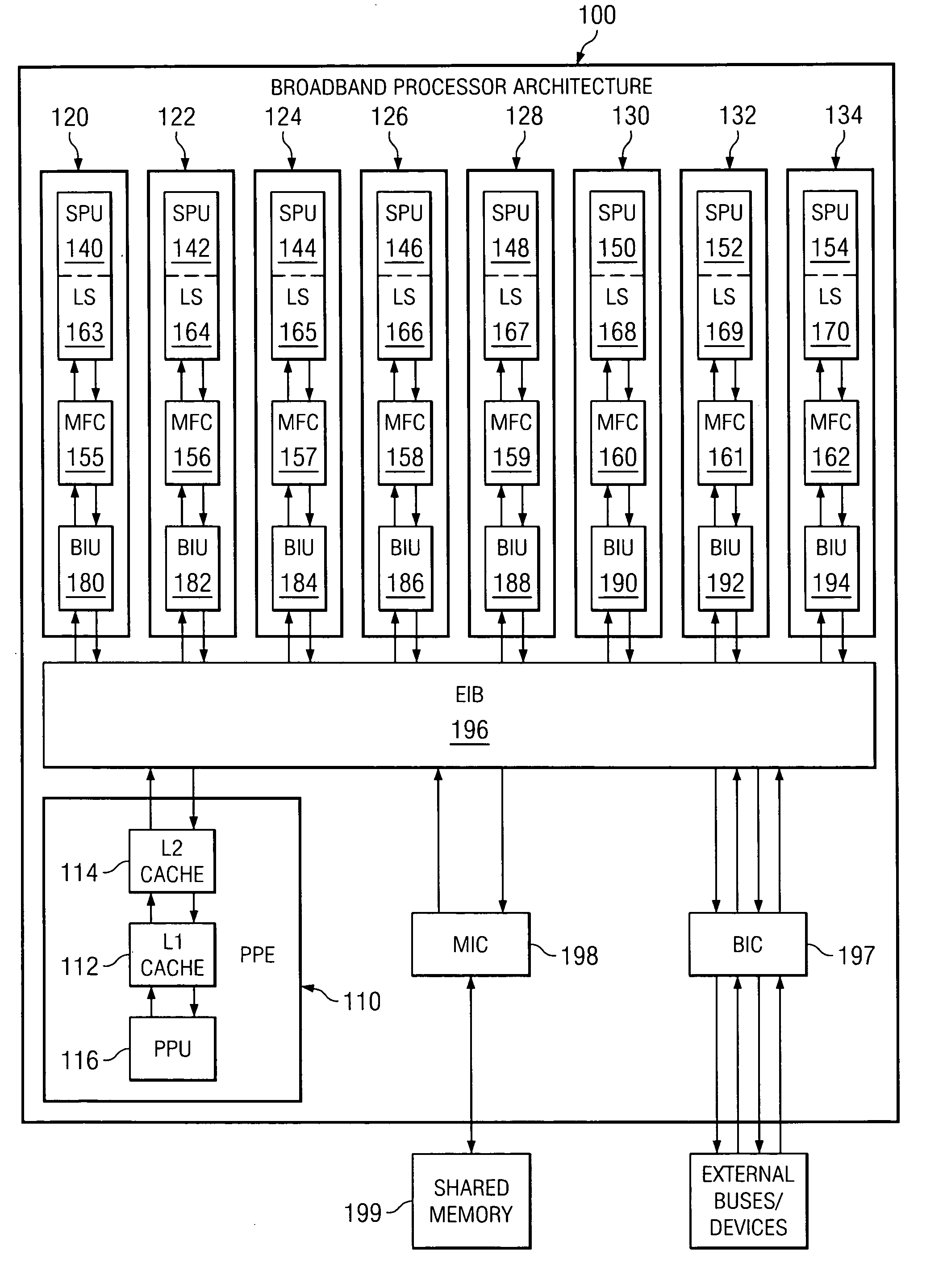
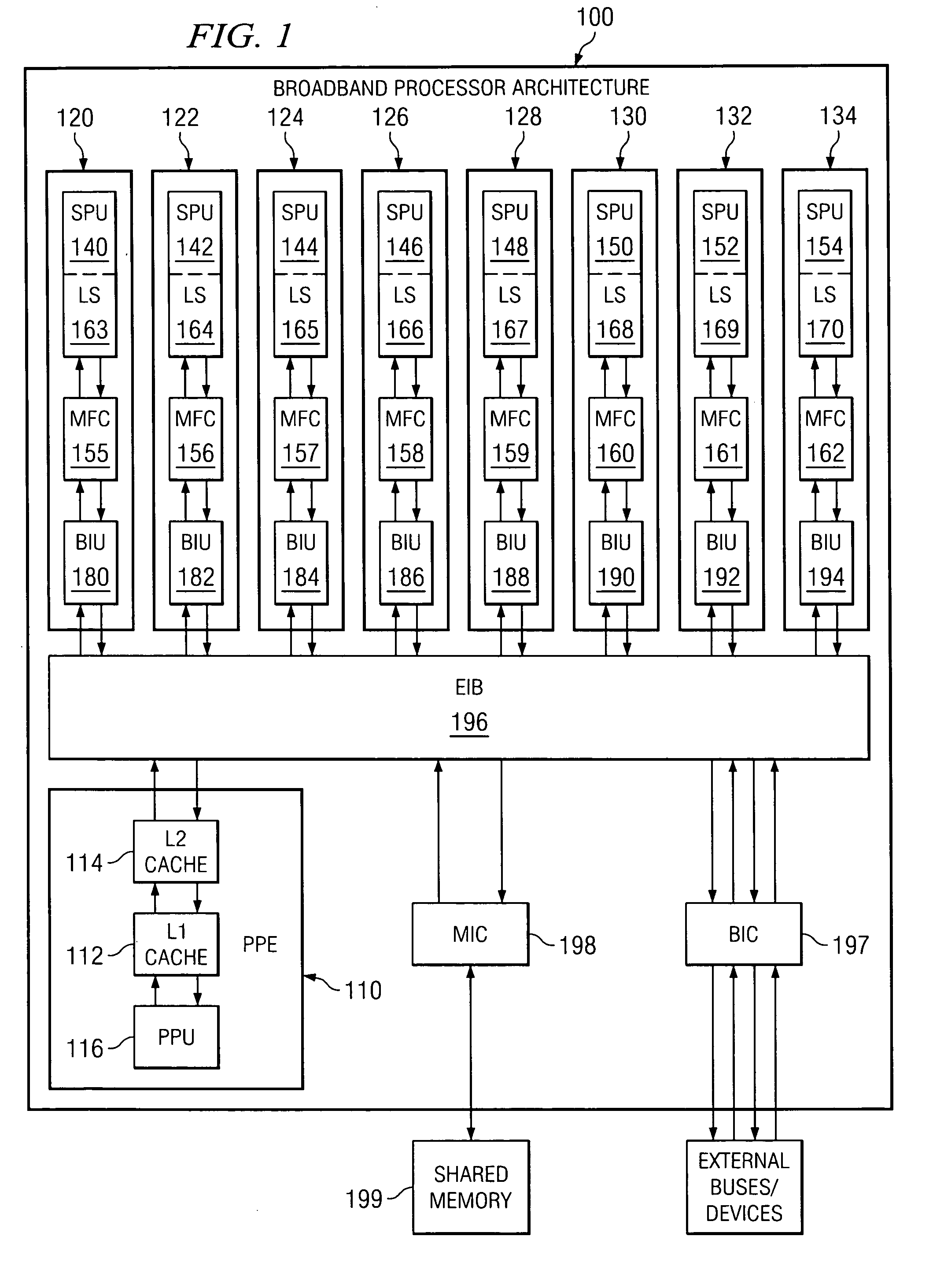
[0040] The present invention provides a high speed on-chip serial link apparatus and method. As such, the present invention is especially well suited for use with integrated circuit chips. In particular, in the exemplary embodiments of the present invention, the high speed on-chip serial link apparatus and method is used for on-chip signal communication in multi-processor microprocessor chips. In one exemplary embodiment, the present invention is implemented with a CELL Broadband Engine Architecture in which there is a power processor element and multiple synergistic processor elements. While this particular architecture will be used to explain the inventive aspects of the present invention, the present invention is not limited to use with such an architecture. To the contrary, the present invention may be used with any integrated circuit chip in which an external, off-chip, peripheral device interface is used to communicate with devices on the chip, without departing from the spiri...


PUM


Abstract

A converter apparatus and method are provided that transforms an external low speed industry standard interface into an on-chip high speed serial link (HSSL). The converter of the present invention is preferably placed in close vicinity of the external interface. The HSSL operates at the system clock speed and, as a result, the HSSL interface signals can be readily treated like any other timed signal facilitating the physical design process. Because synchronization is performed once in the converter near the external interface and the signals along the HSSL of the present invention may be treated like any other timed signal, the need for interface units in each processing element of the chip to perform synchronization is eliminated. Thus, the complexity and silicon area used by the present invention is reduced. The converter enables the maximum speed for the serial interface, which is crucial in power-on-reset, manufacturing testing, and chip debugging.

Description

BACKGROUND OF THE INVENTION [0001] 1. Technical Field [0002] The present invention relates generally to an improved integrated circuit chip. More specifically, the present invention is directed to a high speed on-chip serial link apparatus and method. [0003] 2. Description of Related Art [0004] State-of-the-art very large scale integrated (VLSI) chips need asynchronous serial interfaces to load configuration data for power-on reset, manufacturing test, debugging, and the like. These interfaces typically operate at very low clock frequencies compared to the system clocks and have clock ratios on the order of 100 to 10000 times slower than the system clock cycle, depending on the chosen implementation. These low clock frequencies result in slow power-on sequences, long manufacturing test cycles per chip, and long delays to transfer debug information during the chip “bring-up” phase. [0005] In recent years, more and more stand-alone chips with separate asynchronous serial interfaces ar...

Claims


Application Information

Patent Timeline
IPC IPC(8): G06F3/00
CPCG06F13/4054
Inventor GLOEKLER, TILMANHOLM, INGEMARKOESTER, RALPH C.RILEY, MACK W.
Owner MICROSOFT TECH LICENSING LLC
Why Eureka
Try Eureka