

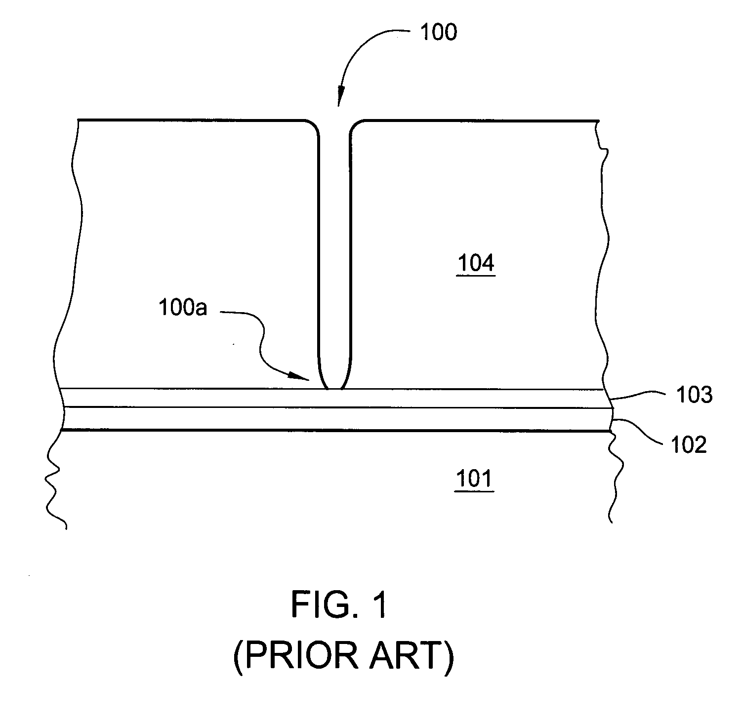
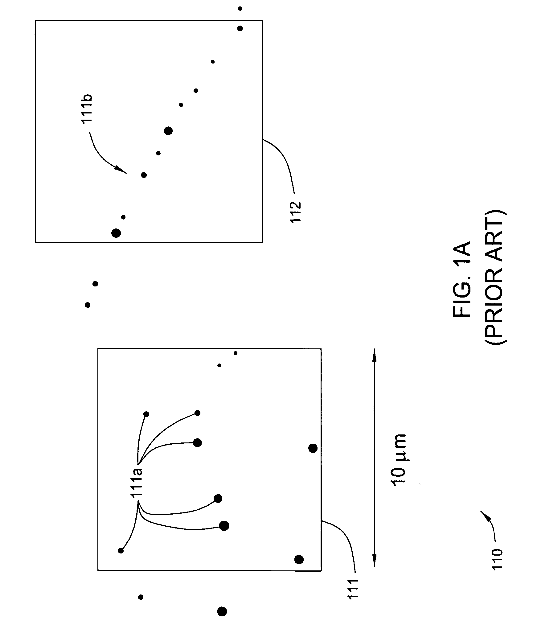
Pre-treatment to eliminate the defects formed during electrochemical plating
a technology of electrochemical plating and pretreatment, which is applied in the direction of superimposed coating process, vacuum evaporation coating, coating, etc., can solve the problems of increasing the current density of such features, not consistently filling structures with narrow openings or difficult aspect ratios, and forming voids in conductors. , to achieve the effect of improving wettability, reducing void defects, and high ra
- Summary
- Abstract
- Description
- Claims
- Application Information
AI Technical Summary
Benefits of technology
Problems solved by technology
Method used
Image

Examples
Embodiment Construction
[0032] Embodiments of the invention generally provide various methods for processing a substrate to reduce the number of void-type defects formed on the substrate when an electrochemical plating process is performed on the substrate. The method of the invention is designed to minimize plating defects by performing one or more preprocessing steps on a substrate prior to performing the ECP process.
[0033]“Plating” as used herein, refers to any deposition process that includes electrochemical plating, electroless plating, or a combination of both.
[0034] Percent concentrations of gas mixtures, as used herein, refer to volume percent.
[0035]“Ambient air” as used herein, refers to air that contains about 21% O2 (by volume). For example, a volume of air that has been sealed in a container that also contains substances that spontaneously react with the gaseous oxygen therein, such as un-oxidized copper, is not considered “ambient air” after any significant period of time has elapsed. This ...
PUM
| Property | Measurement | Unit |
|---|---|---|
| velocity | aaaaa | aaaaa |
| velocity | aaaaa | aaaaa |
| humidity | aaaaa | aaaaa |
Abstract
Description
Claims
Application Information