Display device

a display device and display technology, applied in the field of display devices, can solve the problems of uneven representation, inability to make more than pixel pitch, and non-uniformity in a picture, and achieve the effect of free of uneven representation

Inactive Publication Date: 2007-04-12
SAMSUNG DISPLAY CO LTD +1
View PDF4 Cites 64 Cited by
  • Summary
  • Abstract
  • Description
  • Claims
  • Application Information

AI Technical Summary

Benefits of technology

[0032] The invention has been thought of in order to solve the problems of the above prior art, and has its object to provide a technique for display devices, in which dispersion in representation among a plurality of pixels, attributable to dispersion in characteristics of drive thin-film transistors is decreased and uniform representation free of unevenness can be obtained.
[0033] Also, another object of the invention is to provide a technique capable of decreasing voltage drop and power consumption caused by resistance of taken-out wirings of cathode electrodes in a display device.
[0046] Also, since current from the luminescent elements in all pixels flows through taken-out wirings of cathode electrodes of current drive type luminescent elements arranged in respective pixel regions, it is important to decrease resistance of the taken-out wirings.
[0047] According to the invention, voltage drop and power consumption caused by resistance of taken-out wirings are minimized by shortening lengths of the taken-out wirings, which are connected electrically to cathode electrodes of a plurality of current drive type luminescent elements, extending from an external connection terminal to a contact area.

Problems solved by technology

The two-transistor structured fundamental pixel circuit causes a significant problem that nonuniformity in a picture is caused by dispersion every pixel in a threshold voltage (Vth) and mobility (μ) of the EL drive TFT due to dispersion every location in the crystallizing property of a semiconductor thin film (for which a polycrystal silicon film is ordinarily used) constituting the EL drive TFT.
Such unevenness in representation becomes particularly problematic when a drive current value is small to represent half tone.
However, the prior techniques described above involve the following problems.
However, even when TFT size is increased, it cannot be made greater than pixel pitch.
Accordingly, since a size of an EL drive TFT for driving an EL element, which constitutes each pixel, is limited within an area of a pixel, and the crystallizing property of a polycrystal silicon film disperses every location, it is not possible to compensate for dispersion between the characteristics of an EL drive TFT in a particular pixel and the characteristics of an EL drive TFT in a pixel adjacent the particular pixel.
Accordingly, it is difficult in the second prior technique to obtain a fairly uniform property of representation.
However, known as an essential problem in this driving method is bleeding in a picture generated when animation called pseudo-profile is represented because tone representation is made by luminescence pulse, which is developed on time base.
Also, because of a need for processing a short signal pulse conformed to digital tone, there is caused a problem that the drive circuit is increased in operation frequency and power consumption.
Also, there is also caused a problem that a vertical scanning circuit; which may ordinarily be a simple circuit, becomes complex and a circuit area is increased.
The fourth prior technique is much effective in uniformizing picture representation, but multitone is difficult since it is necessary to form in a unit pixel EL elements having areas conformed to digital tone and to form EL drive TFTs corresponding to the respective EL elements.
In the case of using EL elements having different luminescent areas, deterioration is caused with time beginning with an EL element, which has a small area corresponding to a low-tone bit, thus causing also a problem that normal tone becomes difficult with time.
With the fifth prior technique, the provision of a circuit for canceling dispersion in threshold voltage of an EL drive TFT necessitates a wiring, which is not necessary in a conventional two-transistor configuration, so that a decrease in numerical aperture and yield in manufacture causes a problem.
Therefore, there is caused a problem that no fairly uniformizing effect is obtained on drive current.
However, it is apparent that normal tone representation is made difficult when the plurality of EL drive TFTs disperse in characteristics.
Also, since the plurality of EL drive TFTs are formed in a single pixel in this method, the technique is in no way effective in decreasing dispersion in representation among a plurality of pixels.
With the seventh prior technique, dispersion in drive current can be decreased in the case where one of two EL drive TFTs connected in parallel is varied in characteristics, but dispersion in drive current cannot be decreased in the case where both the two EL drive TFTs are varied in characteristics, and besides the two EL drive TFTs are formed in a single pixel, so that the technique is in no way effective in decreasing dispersion in representation among a plurality of pixels.

Method used


Image

  • Display device
  • Display device
  • Display device

Examples


first embodiment

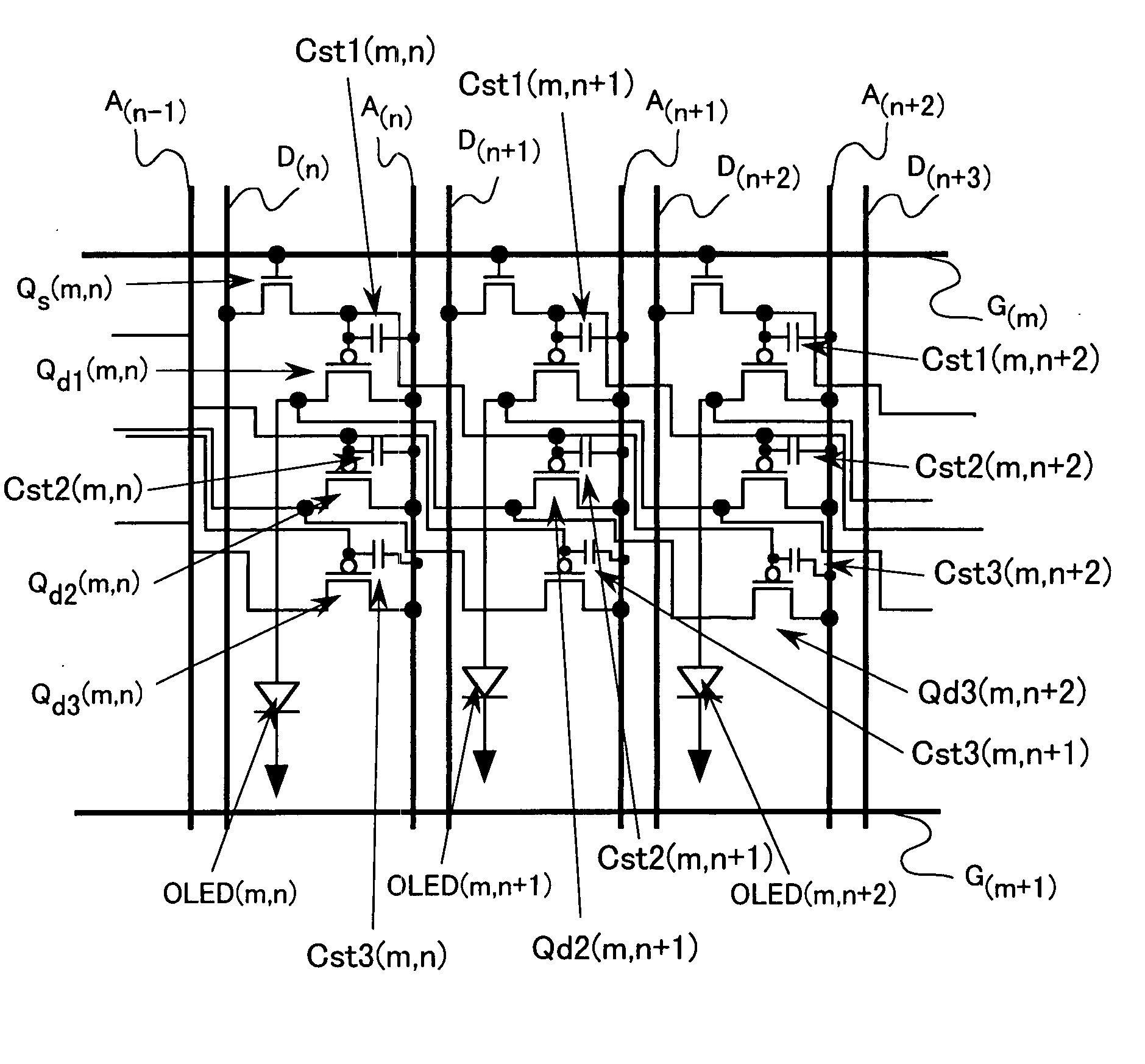
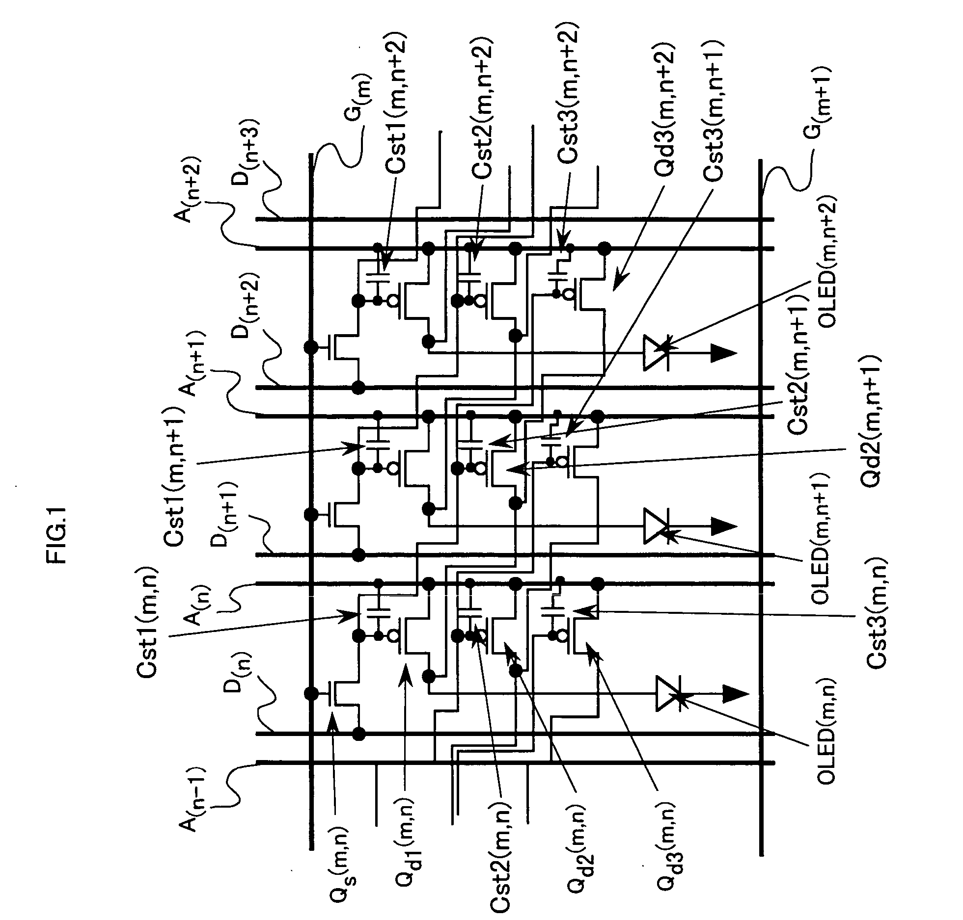
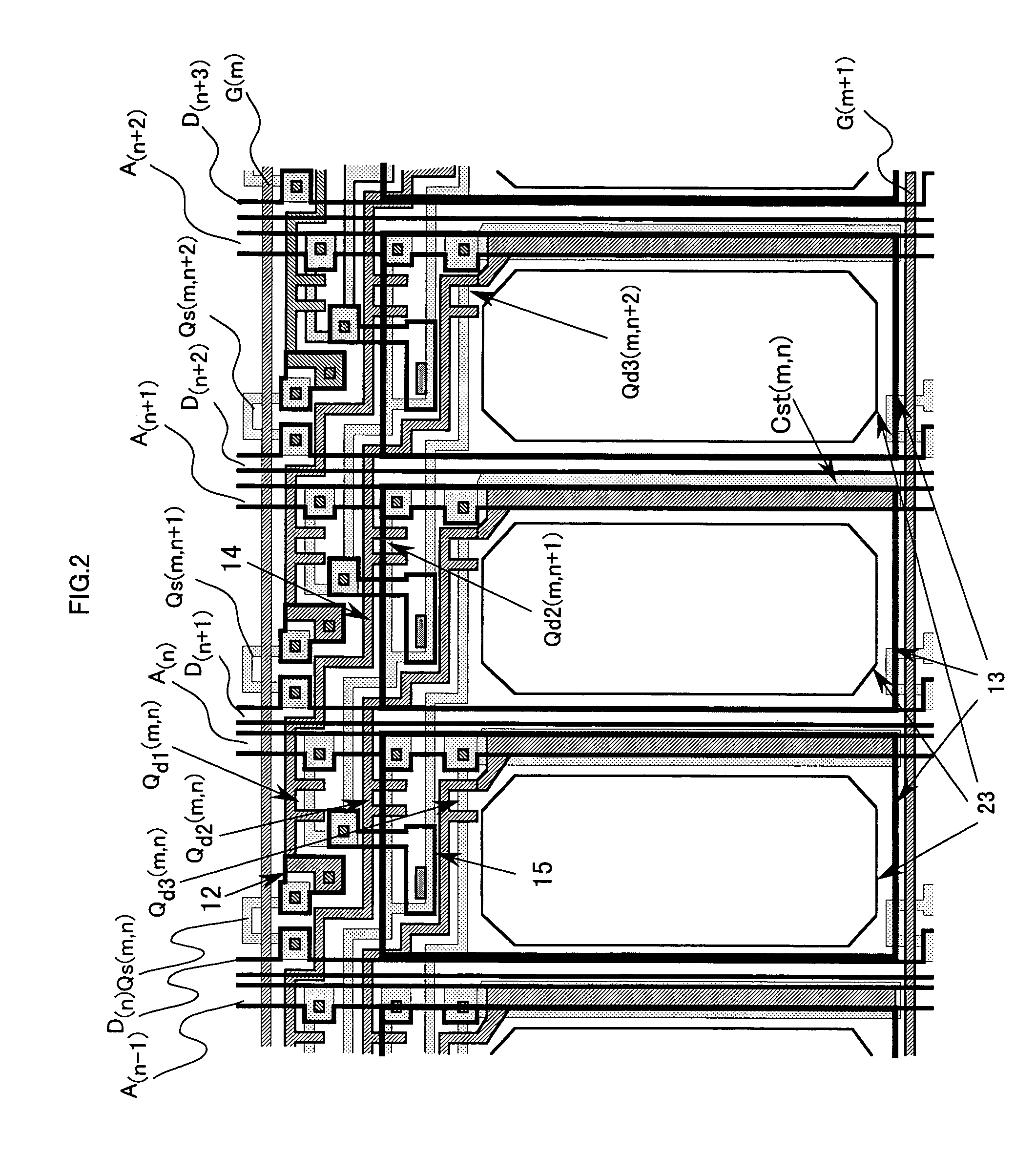
[0078]FIG. 1 is a circuit diagram showing equivalent networks for pixels in a display device according to a first embodiment of the invention, and FIG. 2 is a plan view showing a pixel arrangement in the display device according to the first embodiment of the invention.

[0079] In a self-luminescence display device according to the invention, organic electroluminescent elements (referred simply below to as EL elements) of respective pixels are driven by three drive thin-film transistors (referred below to as EL drive TFT) provided on different pixel regions.

[0080] In the first embodiment, respective EL drive TFTs are arranged in an associated pixel, the next pixel on the right side and the further next pixel but one on the right side.

[0081] In FIG. 1, there are shown three pixel regions surrounded by scanning signal wiring electrodes (Gm, G(m+1)), picture signal wiring electrodes (Dn to D(n+1)), and anode current feeding wiring electrodes (A(n−1) to A(n+2)), which constitute a part...

second embodiment

[0107]FIG. 4 is a circuit diagram showing equivalent networks for pixels in a display device according to a second embodiment of the invention, and FIG. 5 is a plan view showing a pixel arrangement in the display device according to the second embodiment of the invention.

As described above, with the self-luminescence display device according to the invention, EL elements of respective pixels are driven by three EL drive TFTs provided on different pixel regions.

[0108] In the embodiment, respective EL drive TFTs are arranged in an associated pixel, and the next pixels on the right and left sides.

[0109]FIG. 4 shows three regions of pixels surrounded by scanning signal wiring electrodes (Gm, G(m+1)), picture signal wiring electrodes (D(n−1) to D(n+2)), anode current feeding wiring electrodes (A(n−2) to A(n+1)), which constitute a part of the matrix.

[0110] A pixel in row m and column n is defined by a region, which is surrounded by scanning signal wiring electrodes (Gm, G(m+1)), a p...

third embodiment

[0162]FIG. 10 is a circuit diagram showing equivalent networks for pixels in a display device according to a third embodiment of the invention, and FIG. 11 is a plan view showing a pixel arrangement in the display device according to the third embodiment of the invention.

[0163] With the self-luminescence display device according to the embodiment, an EL element OLED(m, n) in row m and column n is driven by five parallel EL drive TFTs formed in total five regions of pixels in row m and column (n−2), row m and column (n−1), row m and column (n+1), and row m and column (n+2) as well as in row m and column n.

[0164] Since the number in parallel is five, such averaging greatly contributes to improvement in uniformity, which makes it possible to obtain an enhanced uniform display characteristics.


PUM


Abstract

A self-luminescence display device, in which dispersion in display among a plurality of pixels, caused by dispersion in characteristics among drive thin-film transistors, is decreased and uniform display free of unevenness can be obtained. The device includes a plurality of pixels having current drive type luminescent elements, and parallel-connected n (n≧2) thin-film transistors to feed a drive current to the respective current drive type luminescent elements. The transistors are arranged in different pixels, respectively, for example, in a first region of pixels adjacent to one another along a first direction. A second region of dummy pixels can be provided on at least one side of said first region along said first direction.

Description

CROSS REFERENCE TO RELATED APPLICATION [0001] This is a divisional of U.S. application Ser. No. 10 / 304,700, filed Nov. 27, 2002. This application relates to and claims priority from Japanese Patent Application No. 2001-363915, filed on Nov. 29, 2001. The entirety of the contents and subject matter of all of the above is incorporated herein by reference.BACKGROUND OF THE INVENTION [0002] 1. Field of the Invention [0003] The present invention relates to a display device and, more particularly, to a structure of an active matrix type organic electroluminescent display. [0004] 2. Description of the Related Art [0005] Active matrix driven organic electroluminescent displays (referred below to as AMOLED) is expected as flat panel displays of the next generation succeeding conventional liquid crystal displays. [0006] Conventionally, a two-transistor structured circuit, as disclosed in JP-A-2000-163014 (first prior technique), comprising a drive thin-film transistor (referred below to as EL...

Claims


Application Information

Patent Timeline
Patent Type & Authority Applications(United States)
IPC IPC(8): G09G3/36G09F9/30H05B33/26G09G3/20G09G3/30G09G3/32G09G3/3233G09G3/3266G09G3/3291H01L21/20H01L21/336H01L21/77H01L21/84H01L27/12H01L27/32H01L29/786H01L31/062H01L51/50H05B33/14H05B44/00
CPCG09G3/3233G09G2300/0852G09G2320/0233H01L27/12H01L27/3223H01L27/3262H01L29/78645H01L2251/5315H10K59/88H10K59/1213H10K2102/3026
Inventor KAWACHI, GENSHIROSATO, TOSHIHIRONISHITANI, SHIGEYUKITOKUDA, NAOKI
Owner SAMSUNG DISPLAY CO LTD
Why Eureka
Try Eureka