
Pattern defect inspection method and apparatus thereof

a technology of defect inspection and defect detection, applied in the field of patent defect inspection methods and apparatus thereof, can solve the problems of reducing the detection efficiency of secondary electrons, requiring long scanning time, and requiring a large amount of equipment, so as to reduce the potential gradient at the boundary of the preliminary electrification region, reduce the irradiation strength, and achieve high speed

Active Publication Date: 2007-04-19
HITACHI HIGH-TECH CORP
View PDF6 Cites 15 Cited by
  • Summary
  • Abstract
  • Description
  • Claims
  • Application Information

AI Technical Summary

Benefits of technology

[0019] More specifically for example, the present invention is configured so that the electrification potential of a specimen may be equalized along with the movement of a stage by: disposing preliminary electrifiers onto a mirror electron imaging type inspection apparatus; then disposing not a grid-shaped electrode but an electrode having a slit-shaped opening as an electrode to control the electrification potential of each preliminary electrifier; and directing the longitudinal direction of the opening to the direction perpendicular to the moving direction of the stage. Further, the present invention is configured so that: the potential gradient at the boundary of the preliminary electrification region may be reduced by decreasing the irradiation strength as the measurement point comes close to the boundary of the preliminary electrification region; and thus sufficient equalization may be obtained by additional preliminary electrification.
[0020] The present invention makes it possible to: form always uniform electrification potential on a wafer; and thereby detect defects of a semiconductor pattern without error at a high speed.

Problems solved by technology

However, since a SEM inspection apparatus is based on a method of focusing an electron beam into a spot and obtaining an image by two-dimensionally scanning the surface of a specimen, when a specimen is inspected with the apparatus, long scanning time is required and thus the apparatus has an essential drawback to the future increase of inspection speed.
However, in the case of a projection type inspection apparatus, a problem is that the distribution of the emission angle of secondary electrons is wide at the time of imaging.
When all of such secondary electrons are taken into an objective lens and focused into an image, a sufficient spatial resolution cannot be obtained due to the aberration of the objective lens.
Therefore, even though a high current electron beam is used for irradiation as an areal beam in order to form an image, the proportion of the secondary electrons capable of actually contributing to the imaging is low and hence a required S / N ratio of an image is hardly obtained.
In the case of using reflection electrons too, the obtained emission amount is smaller by double digit in comparison with the electric current of the irradiation beam and it is difficult to obtain both high defect detection sensitivity and high speed inspection simultaneously with a conventional projection type inspection apparatus.
However, in a mirror electron imaging type inspection apparatus, an irradiation electron beam is mostly repulsed immediately in front of a wafer by field reversing and hence it is impossible to control the electrification of a specimen with the irradiation electron beam.
Such a time constant is sufficiently long in comparison with the time required for obtaining a mirror electron image but is insufficient in comparison with the inspection time of a whole wafer, and thus additional preliminary electrification is required during inspection.
When it is attempted to further increase inspection speed and improve defect detection accuracy in the inspection of a wafer pattern, conventional technologies have had the following problems.
Here, in the case of a mirror electron imaging type inspection apparatus, most part of the irradiation electron beam is repulsed immediately in front of a wafer by field reversing and hence it is impossible to control the electrification of a specimen with the irradiation electron beam.
Furthermore, in the case of the mirror electron imaging method, the required uniformity of the electrification of a specimen surface is as strict as in the range of about plus or minus 0.5 V and sufficient uniformity has not been obtained with a conventional preliminary electrification technology used for a SEM method.
When a conventional preliminary electrification technology is applied to a mirror electron imaging type inspection apparatus, concretely it is estimated that the following problems arise.
In an electrification controller, a problem is that a grid electrode is used as the control electrode and the distribution of electrification potential becomes two-dimensionally uneven.
In the case of applying electrification control by the irradiation of ultraviolet rays or an electron beam through a grid-shaped electrode, the irradiation is not applied to the portions of a wafer corresponding to the grid, and hence the supply of electric charge is insufficient and the portions where an intended electrification potential is not attained are undesirably formed.
Electrification control by preliminary irradiation can be carried out at any time including before or during the inspection of a specimen to be inspected, but it goes without saying that such unevenness of electrification badly affects the inspection accuracy.
When preliminary irradiation is applied during inspection with a preliminary electrifier or the like, the unevenness of electrification increases particularly in the direction perpendicular to the wafer moving direction.
However, with regard to the unevenness in the direction perpendicular to the moving direction, such equalization is not applied and hence the unevenness in electrification potential still remains.
As stated above, a problem has been that an abnormal contrast caused by the unevenness of electrification potential in a mirror electron image is falsely counted as a defect in real inspection and correct inspection is hindered.

Method used


Image

  • Pattern defect inspection method and apparatus thereof
  • Pattern defect inspection method and apparatus thereof
  • Pattern defect inspection method and apparatus thereof

Examples


embodiment 1

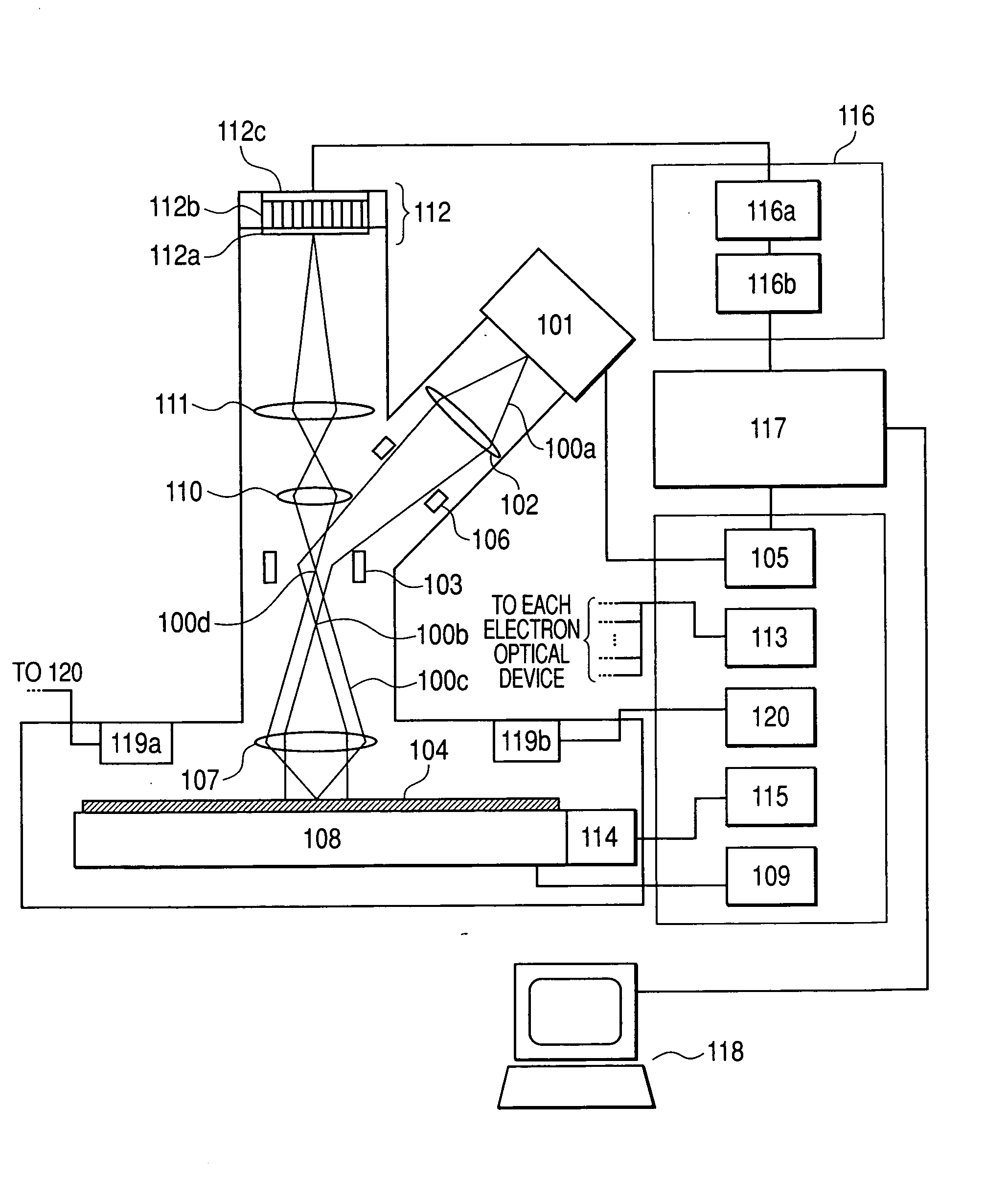
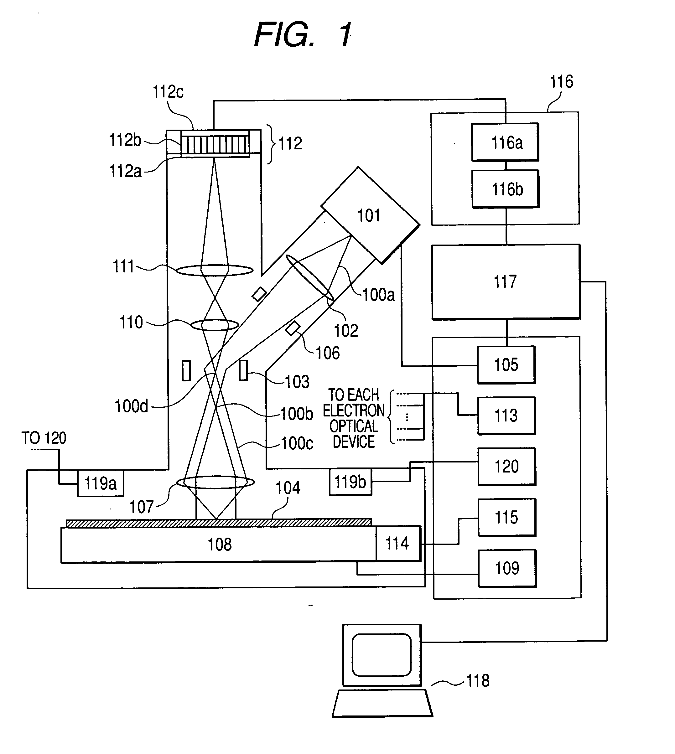
[0039]FIG. 1 shows the outline of a mirror electron imaging type inspection apparatus on which preliminary electrifiers are mounted. Note that a vacuum pump for evacuation, a controller thereof, exhaust pipes, and others are not shown in the figure.

[0040] Firstly, major elements of an electron optical system of the present apparatus are explained. An irradiation electron beam 100a emitted from an electron gun 101: is deflected with an ExB deflector 103 while being converged with a condenser lens 102; forms a crossover 100b; and thereafter is emitted in the form of nearly parallel rays onto a specimen wafer 104. Although the condenser lens 102 is expressed as single lens in the figure, it may also be a system combining plural lenses in order to optimize the optical conditions. In the present embodiment, a Schottky electron source of a Zr—O—W type is used as the electron gun 101. An electron gun using a Zr—O—W type Schottky electron source is suitable for the present apparatus which ...

embodiment 2

[0059] In the present embodiment, an example of an extraction electrode having a structure other than that of a usually used grid electrode in a preliminary electrifier 119 in the apparatus configuration shown in FIG. 1 is explained. FIG. 4 shows a structure of the extraction electrode. The extraction electrode has a lattice structure formed by aligning extra-fine conductive wires 402 in parallel on an opening 401 through which an electron beam passes. The direction of the extension of the wires 402 is the direction (the Y direction) perpendicular to the direction of the movement of a wafer stage during inspection. By mounting the electrode of the present embodiment onto a preliminary electrifier shown in FIG. 1 or FIG. 3a, it is possible to apply electron beam irradiation which is uniform in the direction perpendicular to the direction of the wafer stage movement during inspection to a wafer from the stage of the extraction of the electron beam. As a result, it is possible to form ...

embodiment 3

[0060] There are some cases where a large amount of electric charge must be supplied to a wafer until a desired electrification potential is obtained in accordance with the type of a wafer to be inspected. Since the speed of the wafer stage cannot be changed in the preliminary electrification during inspection, in order to supply a larger amount of electric charge, it is necessary to take a means of either increasing the electric current from an electron source or expanding the irradiation area to the direction of the wafer stage movement. When electric current from an electron source is increased, disadvantages including the shortening of the service life of the electron source and the like tend to arise. To cope with the problem, in the present embodiment, adopted is a structure wherein, in such a preliminary electrifier as shown in FIG. 1 or FIG. 3a, an electrification control electrode 501 and a beam forming slit 502, those being provided with plural openings, are used and thus ...


PUM


Abstract

In the present invention, the structure of an electrification control electrode is changed from a grid type to a slit type and thereby shadows are not formed when a wafer is irradiated with a beam. Further, a beam forming slit is disposed ahead of an electrification control slit, thus the electrification control slit is prevented from being irradiated with an electron beam for preliminary electrification, and thereby secondary electrons which disturb the control of the electrification are inhibited from being generated. The shape of the slit is designed so that the strength of an electron beam may gradually decrease toward both the ends of an electron beam irradiation region in the longitudinal direction thereof. Furthermore, a preliminary static eliminator to remove or reduce the unevenness in an electrification potential distribution which has undesirably been formed earlier is disposed.

Description

CLAIM OF PRIORITY [0001] The present application claims priority from Japanese application JP 2005-174491 filed on Jun. 15, 2005, the content of which is hereby incorporated by reference into this application. FIELD OF THE INVENTION [0002] The present invention relates to a method for inspecting electrical defects of a fine circuit formed on a semiconductor wafer and an apparatus thereof. BACKGROUND OF THE INVENTION [0003] As a method of detecting the defects of a circuit pattern formed on a wafer by comparative inspection of an image in a production process of a semiconductor device, JP-A No. 258703 / 1993, for example, describes a method of comparatively inspecting a pattern by a so-called SEM method wherein an electron beam focused into a spot is used for scanning. The feature of a SEM inspection apparatus is that the resolution thereof is higher than that of an optical inspection apparatus and it can detect electrical defects. However, since a SEM inspection apparatus is based on ...

Claims


Application Information

Patent Timeline
IPC IPC(8): G21K7/00
CPCG01R31/307H01J37/026H01J37/29H01J2237/0045H01J2237/0047H01J2237/045H01J2237/2594H01J2237/2817
Inventor HASEGAWA, MASAKIMAKINO, HIROSHIKOYAMA, HIKARUCHENG, ZHAOHUIMURAKOSHI, HISAYA
Owner HITACHI HIGH-TECH CORP
Learn More