

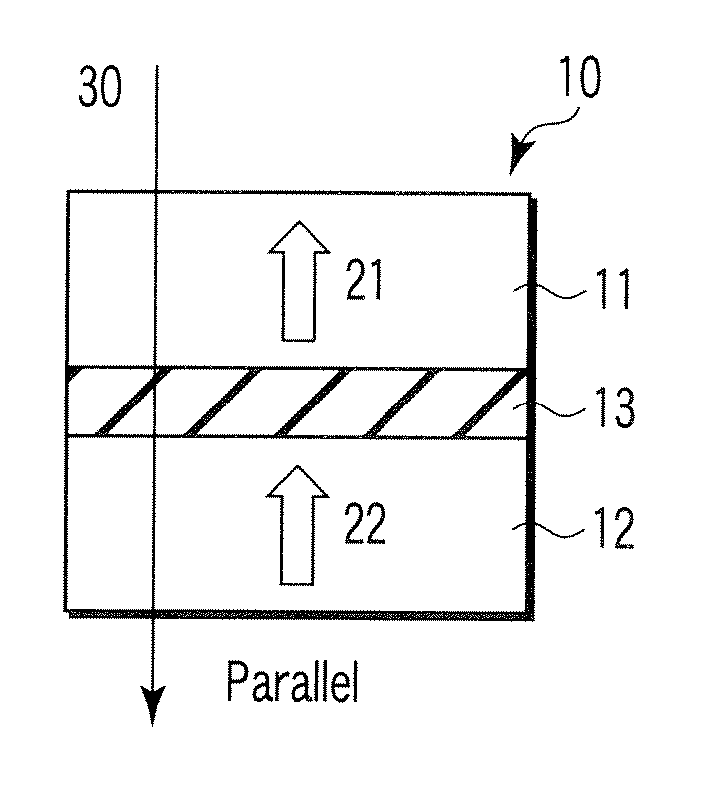
Magnetoresistive element
a random access memory and magnetoresistive element technology, applied in the manufacture of flux-sensitive heads, instruments, record information storage, etc., can solve the problems of limited current that can be supplied to the wiring, and difficult to simultaneously implement both current reduction and microfabrication
- Summary
- Abstract
- Description
- Claims
- Application Information
AI Technical Summary
Benefits of technology
Problems solved by technology
Method used
Image

Examples
example 3
(a) DETAILED EXAMPLE 3
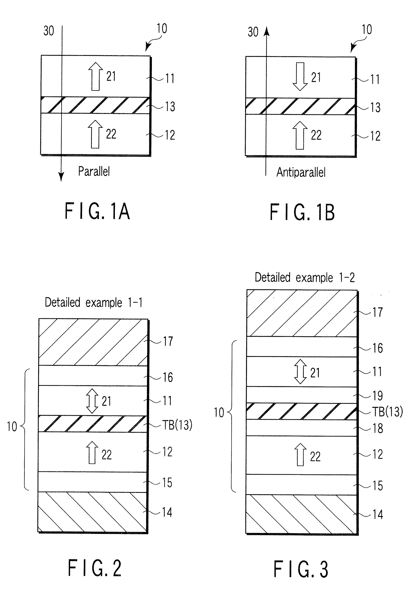
[0161] In an MTJ element of Detailed Example 3, the free layer 11 has an SAF structure, and the magnetization directions of first and second pinned layers 12a and 12b are parallel.
[0162]FIG. 12 is a schematic sectional view showing Detailed Example 3 of the MTJ element according to an embodiment of the present invention. Detailed Example 3 of an MTJ element 10 will be described below.
[0163] As shown in FIG. 12, the MTJ element 10 has a structure in which an underlayer 15, first pinned layer 12a, first highly spin-polarized layer 18, tunnel barrier layer TB, second highly spin-polarized layer 19, free layer 11, second nonmagnetic layer 13b, second pinned layer 12b, and cap layer 16 are stacked in an order named. The free layer 11 has an SAF structure including a first magnetic layer 31, nonmagnetic layer 32, and second magnetic layer 33. A lower electrode 14 is provided on the lower surface of the underlayer 15. An upper electrode 17 is provided on the upper s...
first embodiment
(a) First Embodiment
[0238] The first embodiment is an example of a magnetoresistive random access memory having a select transistor memory cell.
[0239]FIG. 17 is a schematic sectional view showing a magnetoresistive random access memory according to the first embodiment of the present invention. The magnetoresistive random access memory according to the first embodiment will be described below.
[0240] As shown in FIG. 17, a gate insulating film 62 is formed on a semiconductor substrate 61. A gate electrode 63 is formed on the gate insulating film 62. Source / drain diffusion layers 64a and 64b are formed in the semiconductor substrate 61 on both sides of the gate electrode 63. A transistor Tr functioning as a read switching element is thus provided.
[0241] A lead wiring 66 is connected to the drain diffusion layer 64b through a contact 65. A lower wiring 14 is formed on the lead wiring 66. An MTJ element 10 of perpendicular magnetization type is formed on the lower wiring 14. An upper...
second embodiment
(b) Second Embodiment
[0246] When the MTJ element 10 is used, the leakage field from each magnetic layer may influence adjacent cells. In the second embodiment, to reduce the influence of the leakage field, soft magnetic films are provided on wirings.
[0247]FIG. 18 is a schematic sectional view showing a magnetoresistive random access memory according to the second embodiment of the present invention. The magnetoresistive random access memory according to the second embodiment will be described below.
[0248] As shown in FIG. 18, soft magnetic films 71, 72, and 73 are provided on wirings 66, 67, and 69 located on the upper and lower sides of an MTJ element 10. More specifically, the soft magnetic film 73 covers the lower surface of the wiring 67 on the side of the MTJ element 10. The soft magnetic film 72 covers the upper surface of the lead wiring 66 on the side of the MTJ element 10. The soft magnetic film 71 covers the upper surface of the wiring 69 on the side of the MTJ element 1...
PUM
| Property | Measurement | Unit |
|---|---|---|
| aspect ratio | aaaaa | aaaaa |
| magnetocrystalline anisotropy energy density | aaaaa | aaaaa |
| thickness | aaaaa | aaaaa |
Abstract
Description
Claims
Application Information