Ultra shallow junction formation by solid phase diffusion

a technology of solid phase diffusion and ultra-shallow junction, which is applied in the direction of semiconductor devices, electrical apparatus, transistors, etc., can solve the problems of increasing gate to drain overlap capacitance, degrading device performance, and increasing the difficulty of control of ion implantation to form ultra-shallow junctions, for example less than 300 angstroms, so as to improve device performance and reliability, and improve the control of sde or ldd doped region interfaces

Active Publication Date: 2007-04-26
TAIWAN SEMICON MFG CO LTD
View PDF3 Cites 56 Cited by
  • Summary
  • Abstract
  • Description
  • Claims
  • Application Information

AI Technical Summary

Benefits of technology

[0009] To achieve the foregoing and other objects, and in accordance with the purposes of the present invention, as embodied and broadly described herein, an ultra shallow jun

Problems solved by technology

For example, gate to drain overlap capacitance is strongly affected by lateral diffusion of the doped S/D and SDE regions, which is increasingly difficult to control by conventional ion implantation and thermal diffusion processes.
For example, carrying out a process to form raised S/D structures following doping of the S/D regions contributes an additional thermal process which can undesirably increase the lateral diffusion thereby increasing gate to drain overlap capacitance and degrading device performance.
In addition, ion implantation to form ultra-shallow junctions, for example less than about 300 Angstroms, is increasingly difficult to control.
While reducing the ion implant energy may result in shallower junctions,

Method used


Image

  • Ultra shallow junction formation by solid phase diffusion
  • Ultra shallow junction formation by solid phase diffusion
  • Ultra shallow junction formation by solid phase diffusion

Examples


Embodiment Construction

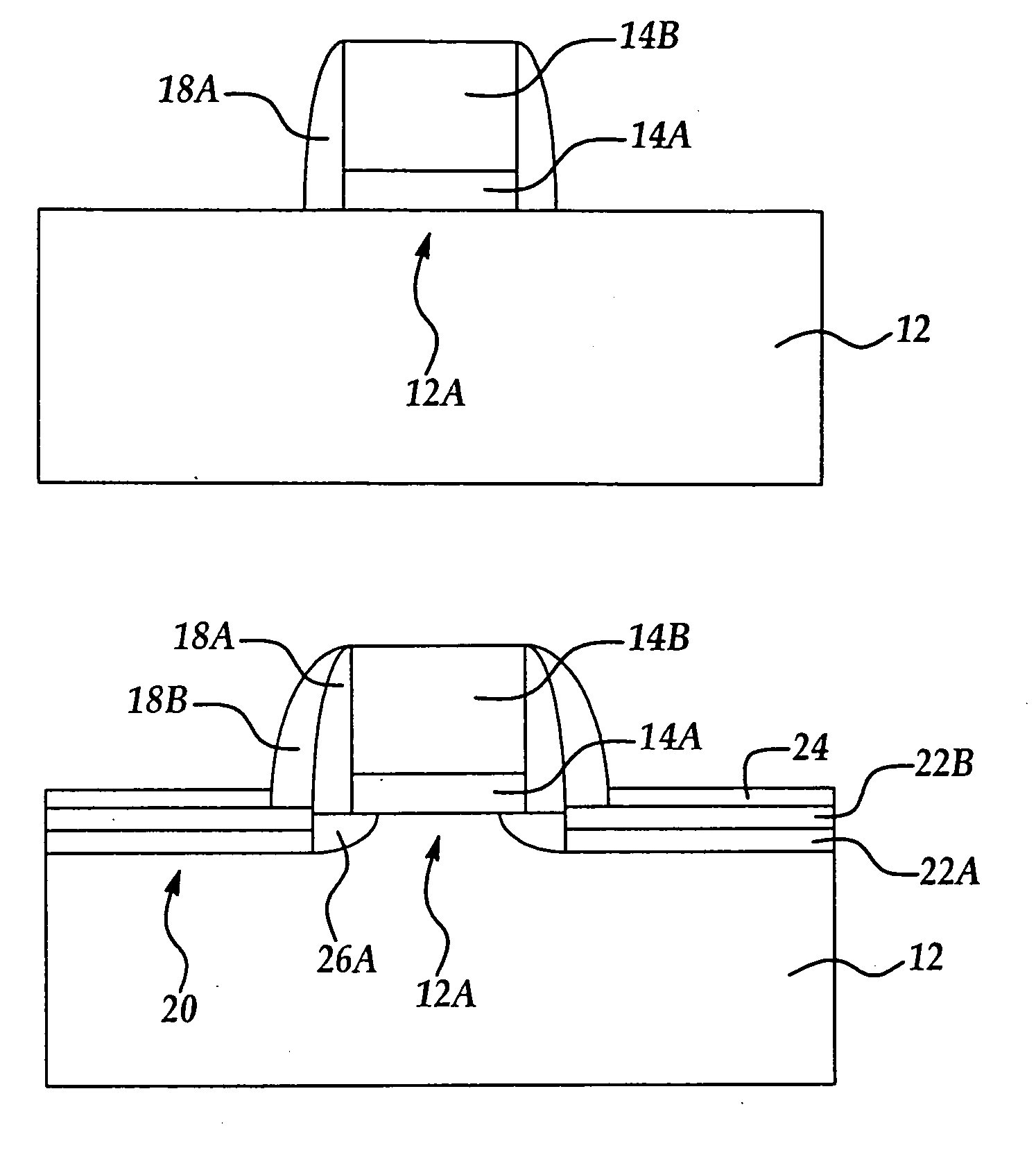
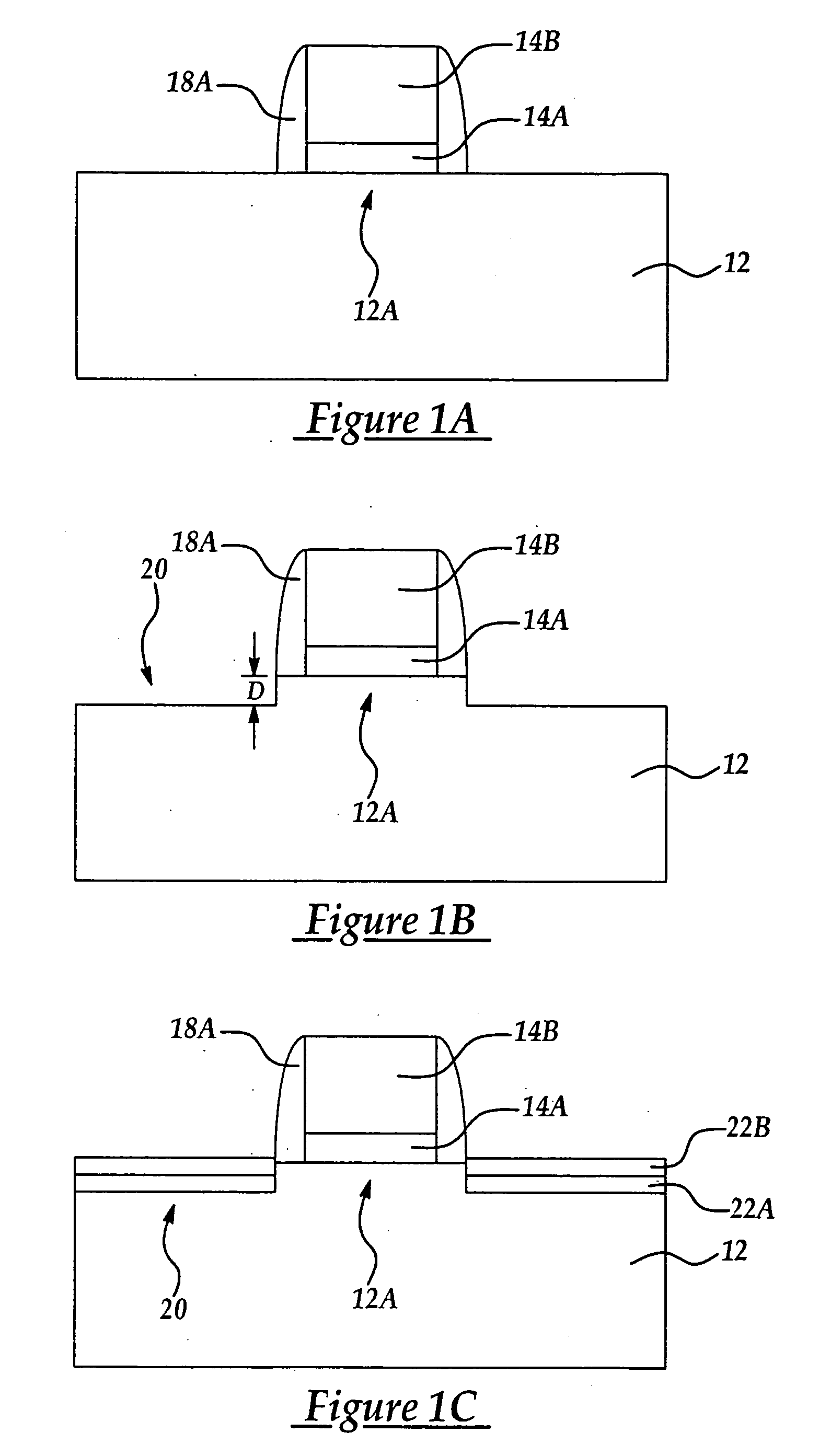
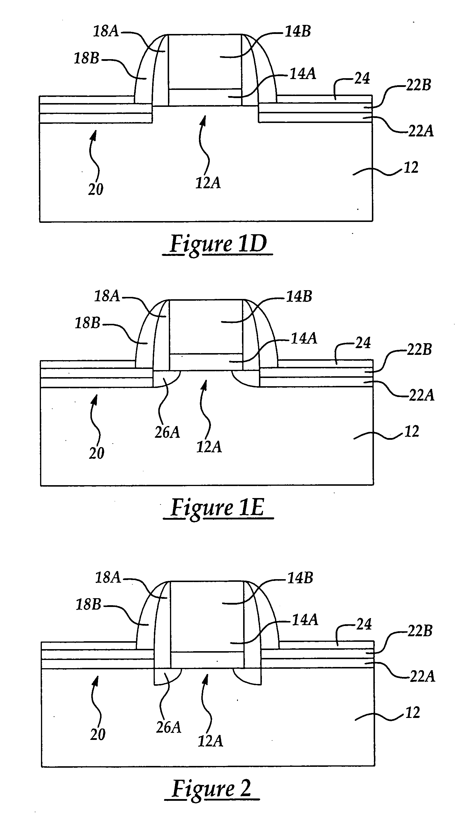
[0015] The method of the present invention is explained with respect to exemplary processing steps for forming ultra-shallow junction (USJ), deep submicron technology MOSFET devices having a junction depth of less than about 200 Angstroms. It will be appreciated that the method may be used with larger device technologies, but that it is most advantageously used with deep sub-micron design rule technologies (e.g., <60 nm), for example where a junction depth is from about 50 to about 200 Angstroms.

[0016] In an exemplary embodiment of the present invention, reference is made to FIGS. 1A-1E where cross sectional schematic views are shown of an exemplary MOSFET device in stages of manufacture according to embodiments of the present invention. For example, referring to FIG. 1A, is shown a semiconductor substrate 12, which may include silicon, strained semiconductor, compound semiconductor, and multi-layered semiconductors, or combinations thereof. For example, the substrate 12 may includ...


PUM


Abstract

An ultra shallow junction (USJ) FET device and method for forming the same with improved control over SDE or LDD doped region interfaces to improve device performance and reliability is provided, the method including providing a semiconductor substrate; forming a gate structure comprising a gate dielectric, an overlying gate electrode, and first offset spacers adjacent either side of the gate electrode; forming at least one doped semiconductor layer comprising dopants over a respective source and drain region adjacent the respective first offset spacers; forming second offset spacers adjacent the respective first offset spacers; and, thermally treating the at least one semiconductor layer to cause out-diffusion of the dopants to form doped regions in the semiconductor substrate.

Description

FIELD OF THE INVENTION [0001] This invention generally relates to MOSFET semiconductor devices and methods for forming the same and more particularly to a MOSFET device and method for forming the same including ultra-shallow junction (USJ) formation by solid phase diffusion (SPD) to reduce short channel effects (SCE) such as drain to gate overlap capacitance and current (diode) leakage characteristics for deep-submicron MOSFET semiconductor devices. BACKGROUND OF THE INVENTION [0002] In the integrated circuit industry today, hundreds of thousands of semiconductor devices are built on a single chip. As the size of CMOS transistors, also referred to as MOSFETs, are scaled down, one of the most important challenges facing a device designer are short channel effects (SCE) in reduced gate length devices. For example, short channel effects that influence the electrical operating characteristics of FET devices include VT rolloff, drain induced barrier lowering (DIBL), subthreshold swing de...

Claims


Application Information

Patent Timeline
IPC IPC(8): H01L21/336
CPCH01L29/165H01L29/517H01L29/6656H01L29/6659H01L29/66628H01L29/66636H01L29/7833
Inventor WANG, CHIH-HAOWANG, YEN-PINGTING, STEVE MINGHUANG, YI-CHUN
Owner TAIWAN SEMICON MFG CO LTD
Why Eureka
Try Eureka