Low Voltage Drop and High Thermal Performance Ball Grid Array Package

a grid array and low voltage drop technology, applied in the direction of semiconductor devices, semiconductor/solid-state device details, electrical apparatus, etc., can solve the problems of reducing the thermal connection between the ic die and the edge of the stiffener, reducing the thermal connection reducing the inductance and voltage drop of the package. , to achieve the effect of improving the thermal conduction of the ic die, reducing the inductance and voltage drop of the package, and

Inactive Publication Date: 2007-05-17
AVAGO TECH WIRELESS IP SINGAPORE PTE
View PDF2 Cites 68 Cited by
  • Summary
  • Abstract
  • Description
  • Claims
  • Application Information

AI Technical Summary

Benefits of technology

[0016] The present invention provides for improved thermal conduction from an IC die and for reduced package inductance and voltage drop. In embodiments of the present invention, a heat sink assembly is coupled in an integrated circuit package. The package may be a land grid array (LGA), pin grid array (PGA), chip scale package (CSP), ball grid array (BGA), quad flat pack (QFP), and other integrated circuit package type. The heat sink assembly provides an enhanced thermal and electrical connection from the IC die to the package substrate.
[0029] In aspects of the present invention, the heat sink assembly provides for an improved thermal conduction path from the IC die. Heat from the IC die may be better conducted to the package substrate by the heat sink assembly, and better radiated to the environment by the heat sink assembly. In a first aspect, a thermal path is formed from the IC die, through the first heat sink element and second heat sink element, to the package substrate. In a second aspect, a thermal path is formed from the IC die, through the single heat sink element, to the package substrate.

Problems solved by technology

Existing BGA packages are subject to high thermal stresses that result from the heat given off during operation of the mounted IC die.
As a result, conventional flex BGA packages have difficulty in meeting reliability requirements for die sizes larger than about 9 mm.
However, the openings on the stiffener for wire bond connections tend to reduce the thermal connections between the IC die and the edges of the stiffener.
As a result, heat spreading is limited largely to the region of the IC die attach pad, while areas at the stiffener periphery do not contribute effectively to heat spreading.
Furthermore, because of the high density of the substrate routing circuitry, it is difficult to bond each power and ground pad on the IC die to the substrate by a corresponding bond finger.
As a result, the distribution of ground and power signals connecting to the IC die is frequently compromised in conventional BGA packages.
The cost of the PBGA package, however, will increase with the number of thermal balls.
Furthermore, a large array of thermal balls may be necessary for heat dissipation into the PCB for high levels of IC device power.
Existing BGA packages have limitations that affect their ability to be used for advanced IC die applications.
These design techniques, however, have limitations.
For example, these design techniques may lead to unwanted BGA package voltage dropping, which can cause poor performance for the packaged IC die.

Method used


Image

  • Low Voltage Drop and High Thermal Performance Ball Grid Array Package
  • Low Voltage Drop and High Thermal Performance Ball Grid Array Package
  • Low Voltage Drop and High Thermal Performance Ball Grid Array Package

Examples


Embodiment Construction

Overview

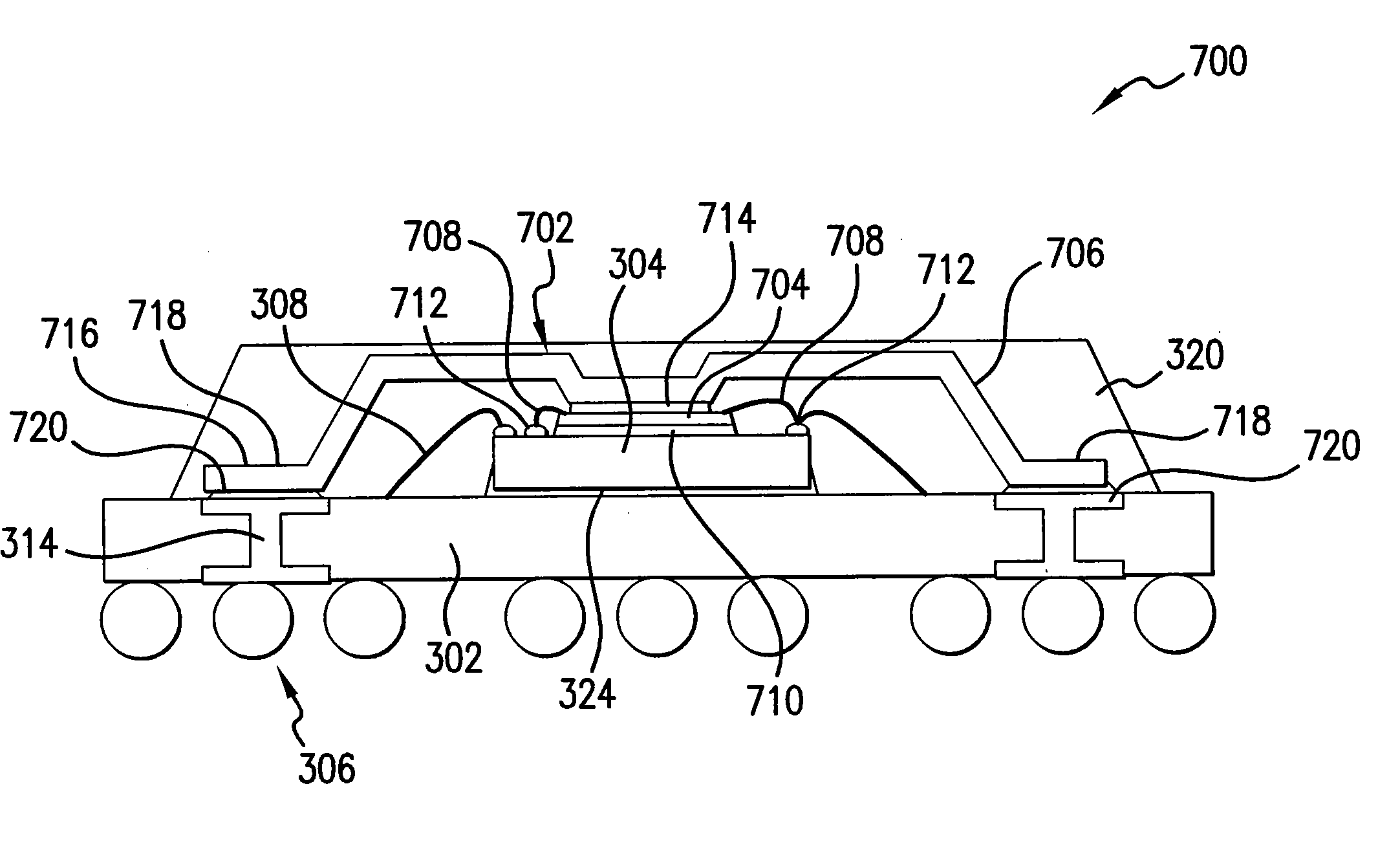
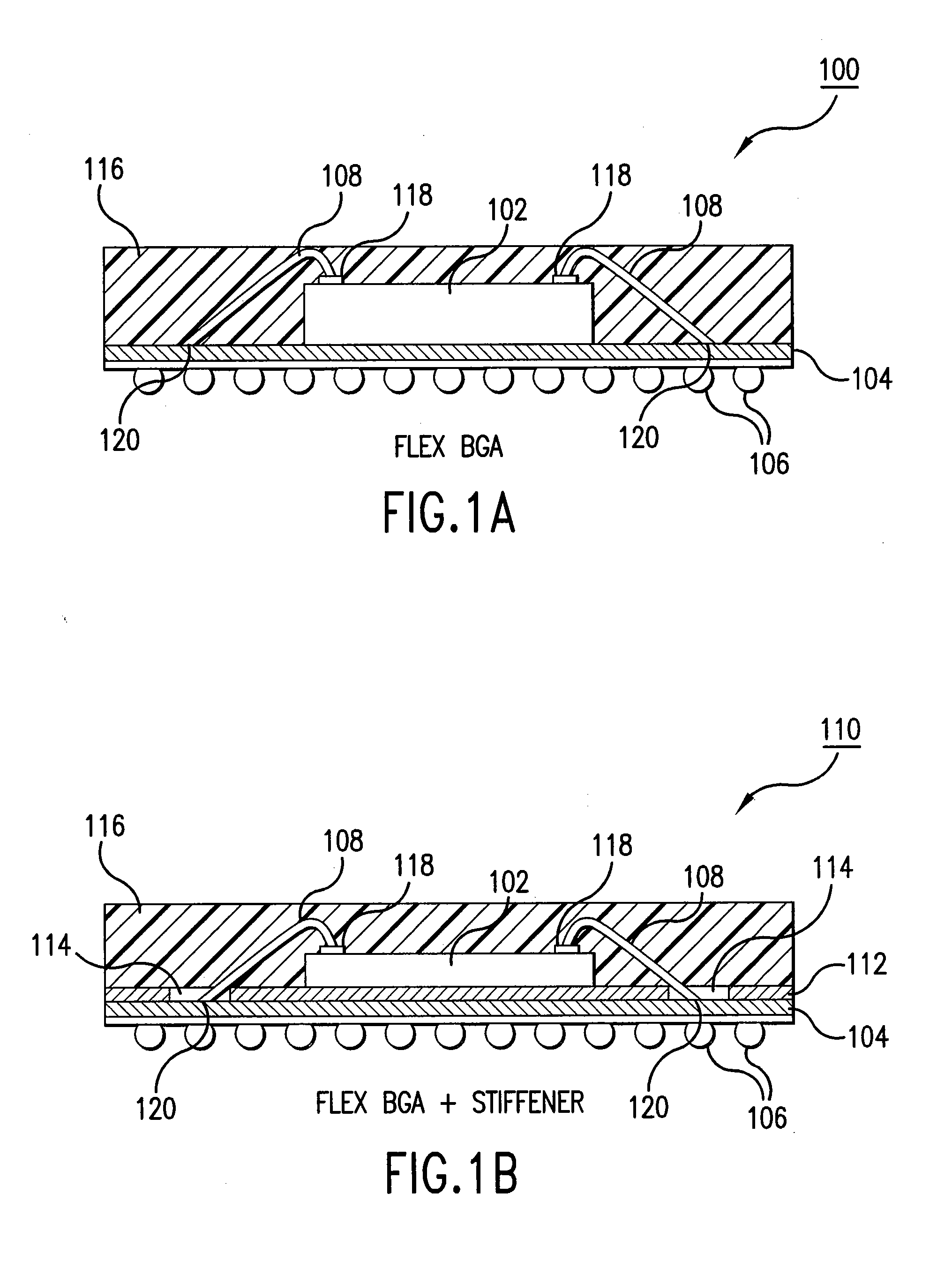
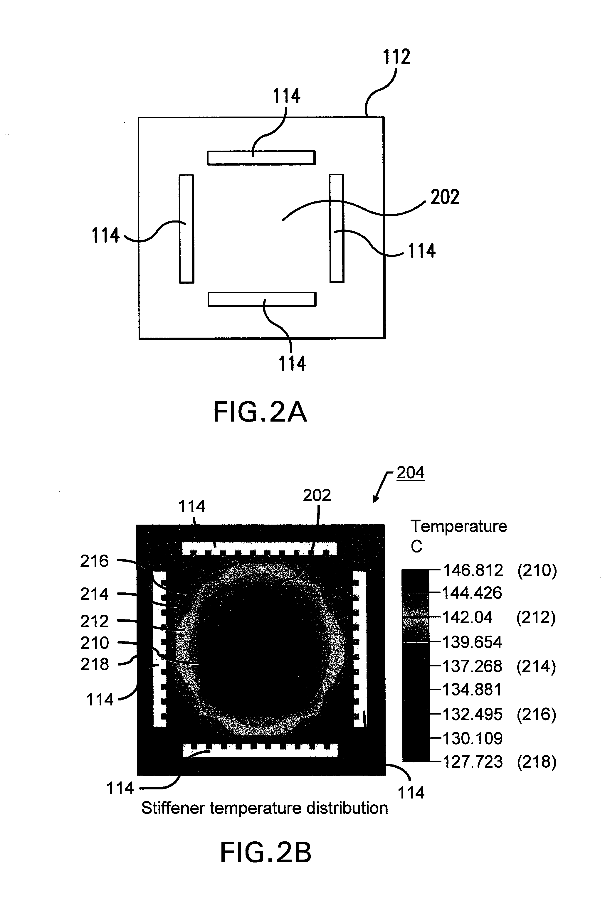
[0064] The present invention is directed to a method, system, and apparatus for improving the mechanical, thermal, and electrical performances of integrated circuit packages. For example, the present invention is applicable in land grid array (LGA), pin grid array (PGA), chip scale package (CSP), ball grid array (BGA), quad flat pack (QFP), and other integrated circuit package types. The present invention is applicable to all types of package substrates, including ceramic, plastic, and tape (flex) substrates. Furthermore the present invention is applicable to die-up (cavity-up) and die-down (cavity-down) IC die orientations. For illustrative purposes, the present invention is described herein as being implemented in a BGA package. However, the present invention is applicable to the other integrated circuit package types mentioned herein, and to additional integrated circuit package types.

[0065] Ball grid array package types are described below. A discussion of package ind...


PUM


Abstract

An apparatus and method for a low voltage drop and thermally enhanced integrated circuit (IC) package are described. A substantially planar substrate having a plurality of contact pads on a first surface is electrically connected through the substrate to a plurality of solder ball pads on a second surface of the substrate. An IC die having a first surface is mounted to the first surface of the substrate. The IC die has a plurality of I / O pads electrically connected to the plurality of contact pads on the first surface of the substrate. A heat sink assembly is coupled to a second surface of the IC die and to a first contact pad on the first surface of the substrate to provide a thermal path from the IC die to the first surface of the substrate. The heat sink assembly can also provide an electrical path from the IC die to the first surface of the substrate. The heat sink assembly may have one or two heat sink elements to provide thermal and / or electrical connectivity between the IC die and the substrate.

Description

CROSS-REFERENCE TO RELATED APPLICATIONS [0001] This application is a continuation of U.S. application Ser. No. 10 / 253,600, filed Sep. 25, 2002, now allowed, which claims the benefit of U.S. Application No. 60 / 366,241, filed Mar. 22, 2002, which are both herein incorporated by reference in their entirety.BACKGROUND OF THE INVENTION [0002] 1. Field of the Invention [0003] The invention relates generally to the field of integrated circuit (IC) device packaging technology and, more particularly, to techniques for improving electrical and thermal performances of ball grid array (BGA) packages. [0004] 2. Background Art [0005] Integrated circuit (IC) dies are typically mounted in or on a package that is attached to a printed circuit board (PCB). One such type of IC die package is a ball grid array (BGA) package. BGA packages provide for smaller footprints than many other package solutions available today. A BGA package has an array of solder balls located on a bottom external surface of a ...

Claims


Application Information

Patent Timeline
Patent Type & Authority Applications(United States)
IPC IPC(8): H01L23/34H01L23/31H01L23/433H01L25/065
CPCH01L23/3128H01L24/49H01L25/0657H01L2224/48091H01L2224/48227H01L2224/48228H01L2224/49171H01L2924/01077H01L2924/01079H01L2924/14H01L2924/1433H01L2924/15311H01L2924/16152H01L2924/30107H01L2924/3011H01L2924/3025H01L2224/73265H01L2224/32225H01L24/48H01L23/4334H01L2924/00014H01L2924/00H01L2924/00012H01L24/73H01L2924/181H01L2224/05599H01L2224/45099H01L2224/85399H01L2224/05554H01L2924/10162H01L2224/45015H01L2924/207
Inventor ZHONG, CHONGHUAKHAN, REZA-UR RAHMAN
Owner AVAGO TECH WIRELESS IP SINGAPORE PTE
Why Eureka
Try Eureka