

Strained-silicon CMOS device and method
- Summary
- Abstract
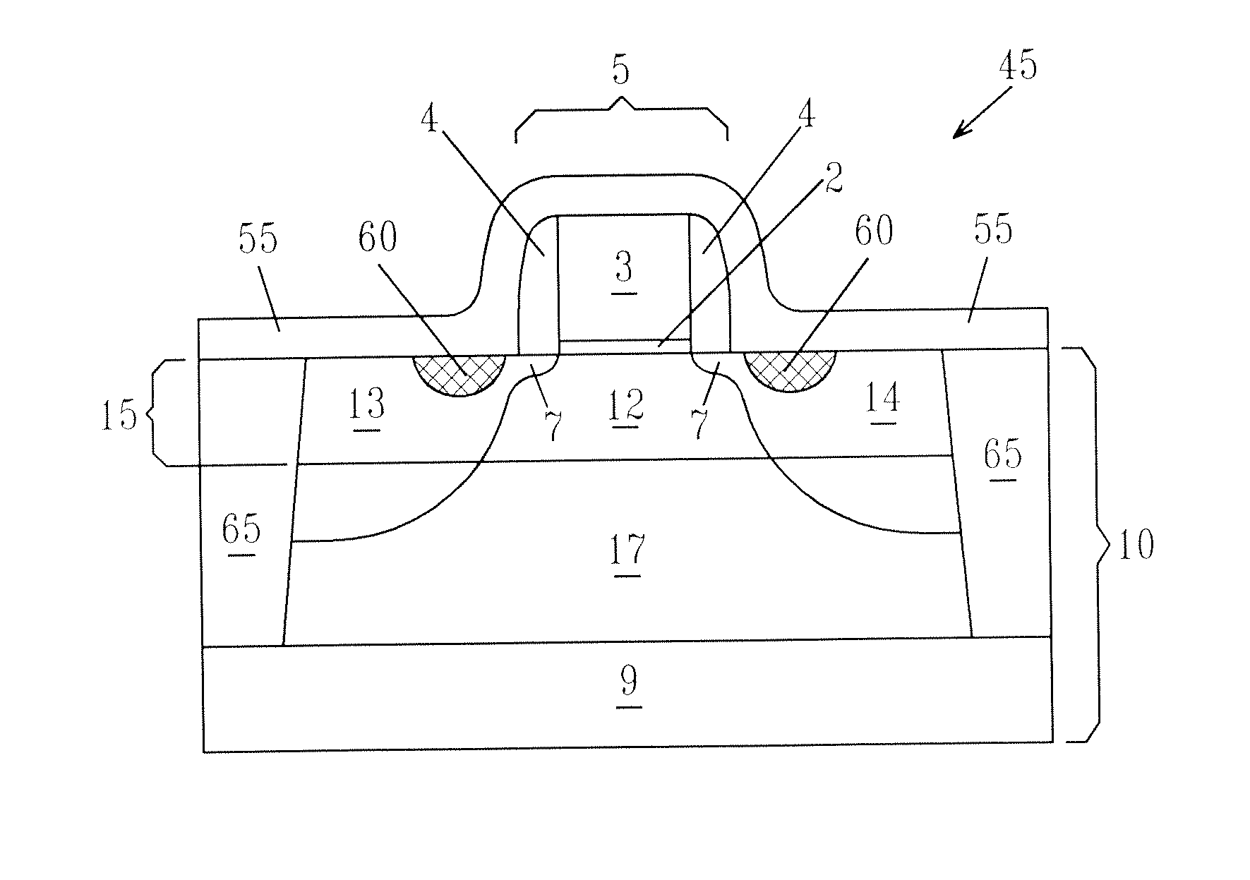
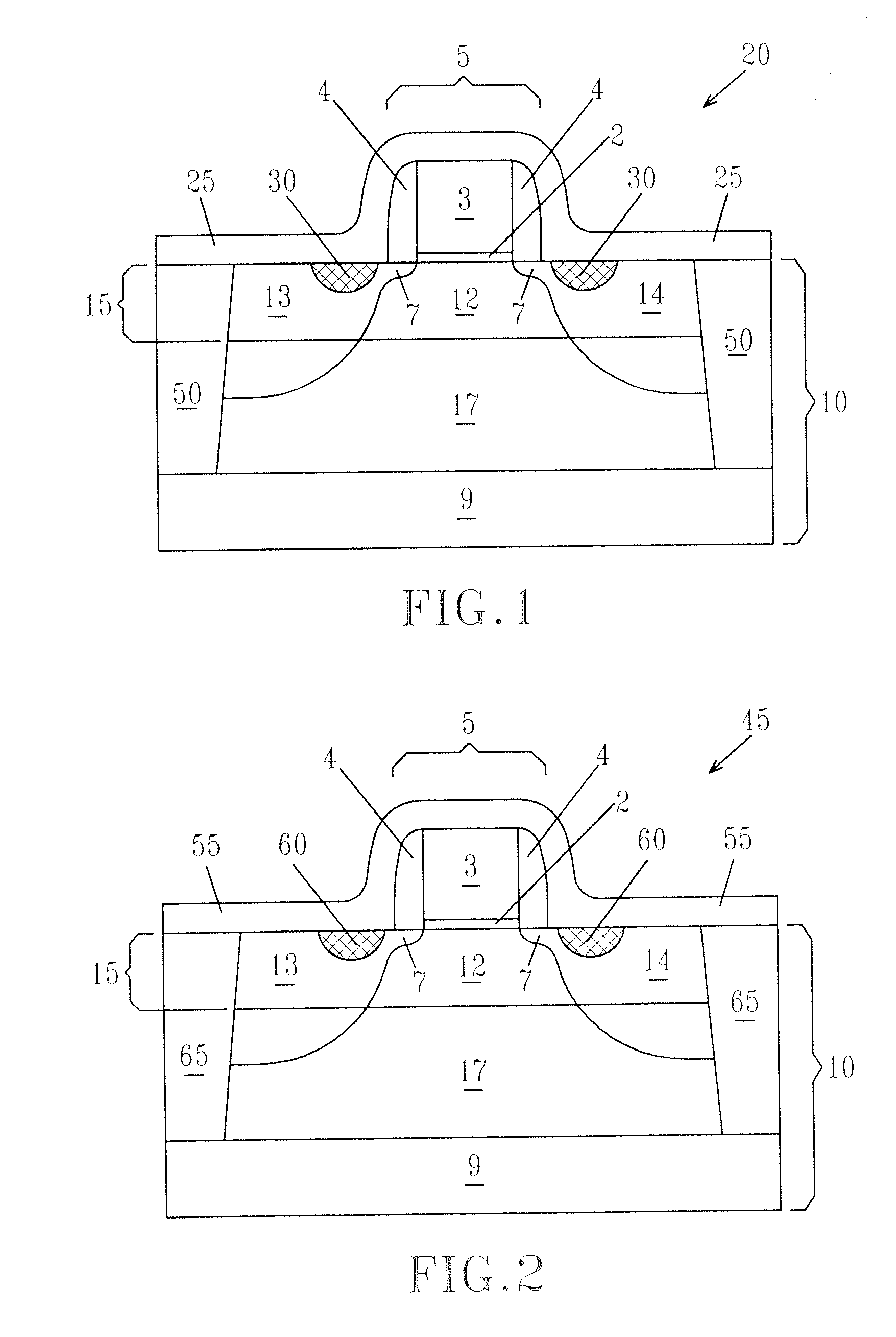
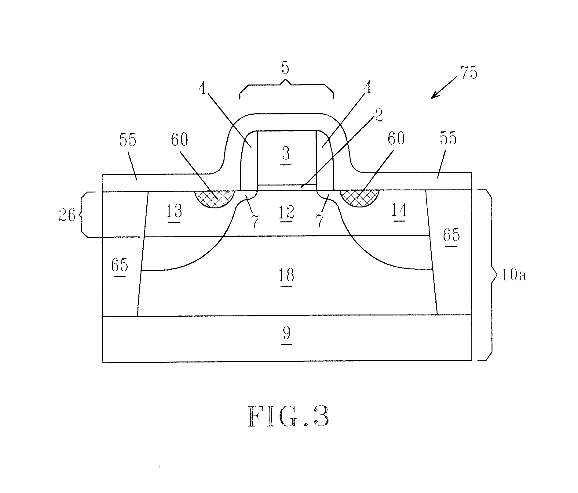
- Description
- Claims
- Application Information
AI Technical Summary
Benefits of technology
Problems solved by technology
Method used
Image

Examples
example 1
Formation of Compressive or Tensile Dielectric Capping Layer atop Biaxially Strained SGOI Substrate
[0138] In this example, a dielectric capping layer (compressive or tensile strain inducing layer) was used to enhance the drive current by introducing a uniaxial strain along the FET channel. When such a dielectric capping layer is deposited over an SGOI FET, the lattice structure was distorted in response to the combination of a biaxial tensile strain and a smaller uniaxial tensile or compressive stress. FIG. 9(a) depicts a schematic description of biaxial tension strained Si, in which the longitudinal lattice dimension (x-direction, parallel to the channel) was equal to the transverse lattice dimension (y-direction, in the same plane and perpendicular to the device channel) and the normal lattice dimension (z-direction, out of the channel plane). FIG. 9(b) depicts the lattice symmetry of the biaxial tension strained Si substrate depicted in FIG. 9(a) with a superimposed uniaxial ten...
PUM
 Abstract
Description
Claims
Application Information