Fabrication of local damascene finFETs using contact type nitride damascene mask

a damascene and damascene technology, applied in the direction of semiconductor devices, basic electric elements, electrical equipment, etc., can solve the problems of degrading other parametric and/or operating characteristics of the resulting devices, increasing leakage, and increasing doping, so as to reduce the defect of gate electrode formation, improve the removal of gate electrode material, and reduce the effect of overetching

Inactive Publication Date: 2007-05-17
SAMSUNG ELECTRONICS CO LTD
View PDF11 Cites 53 Cited by
  • Summary
  • Abstract
  • Description
  • Claims
  • Application Information

AI Technical Summary

Benefits of technology

[0015] Example embodiments include methods of fabricating semiconductor devices that provide for improved removal of the gate electrode material, particularly in those regions separating adjacent fins in a longitudinal direction, thereby allowing for reduced overetching and/or reduced defects during gate electrode for...

Problems solved by technology

Reducing the channel length of planar transistors to levels below about 100 nm, however, also tends to degrade other parametric and/or operating characteristics of the resulting devices.
One particular issue associated with short channel devices include increased leakage as a result of the decreased distance between the corresponding source and drain regions provided on opposite sides of the gate electrode.
One approach for addressing these issues involves increasing the doping level of the channel regions, but, while tending to reduce leakage, the increased doping tends to degrade the active switching function of the transistor.
As a result, the overall performance of the resulting MOSFET device may be severely degraded by these short channel effects (SCE) resulting, for example, in increased leakage currents and less stable and uniform sub-threshold voltages.
Accordingly, the threshold voltage of such finFET transistors cannot be effectively controlled using body-bias, thereby complicating efforts to control the threshold voltage of the resulting CMOS transistors.
However, if a conventional bulk substrate is used to allow for more effective body-bias control, the resulting increase in the extent of the drain depletion region ten...

Method used


Image

  • Fabrication of local damascene finFETs using contact type nitride damascene mask
  • Fabrication of local damascene finFETs using contact type nitride damascene mask
  • Fabrication of local damascene finFETs using contact type nitride damascene mask

Examples


Embodiment Construction

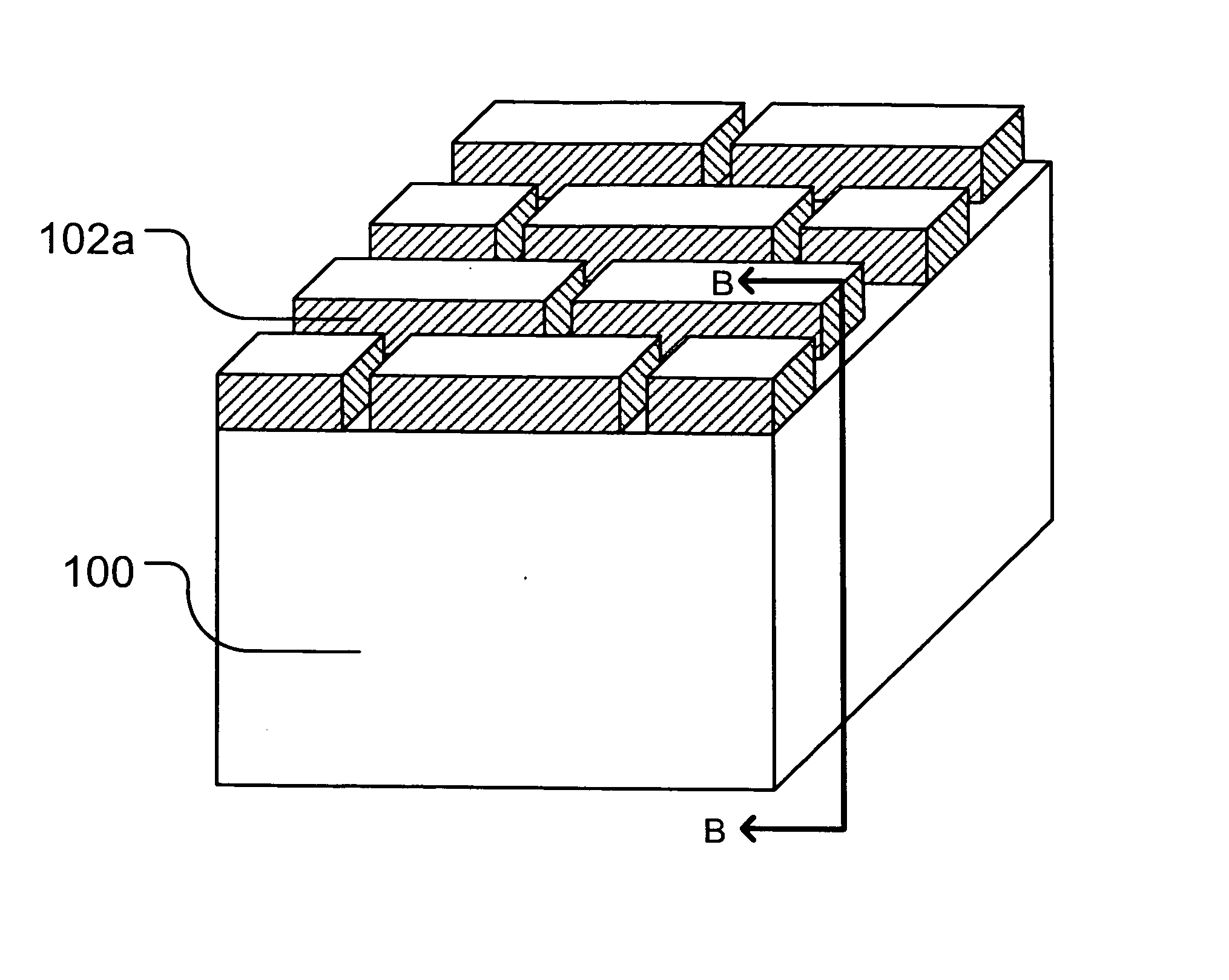
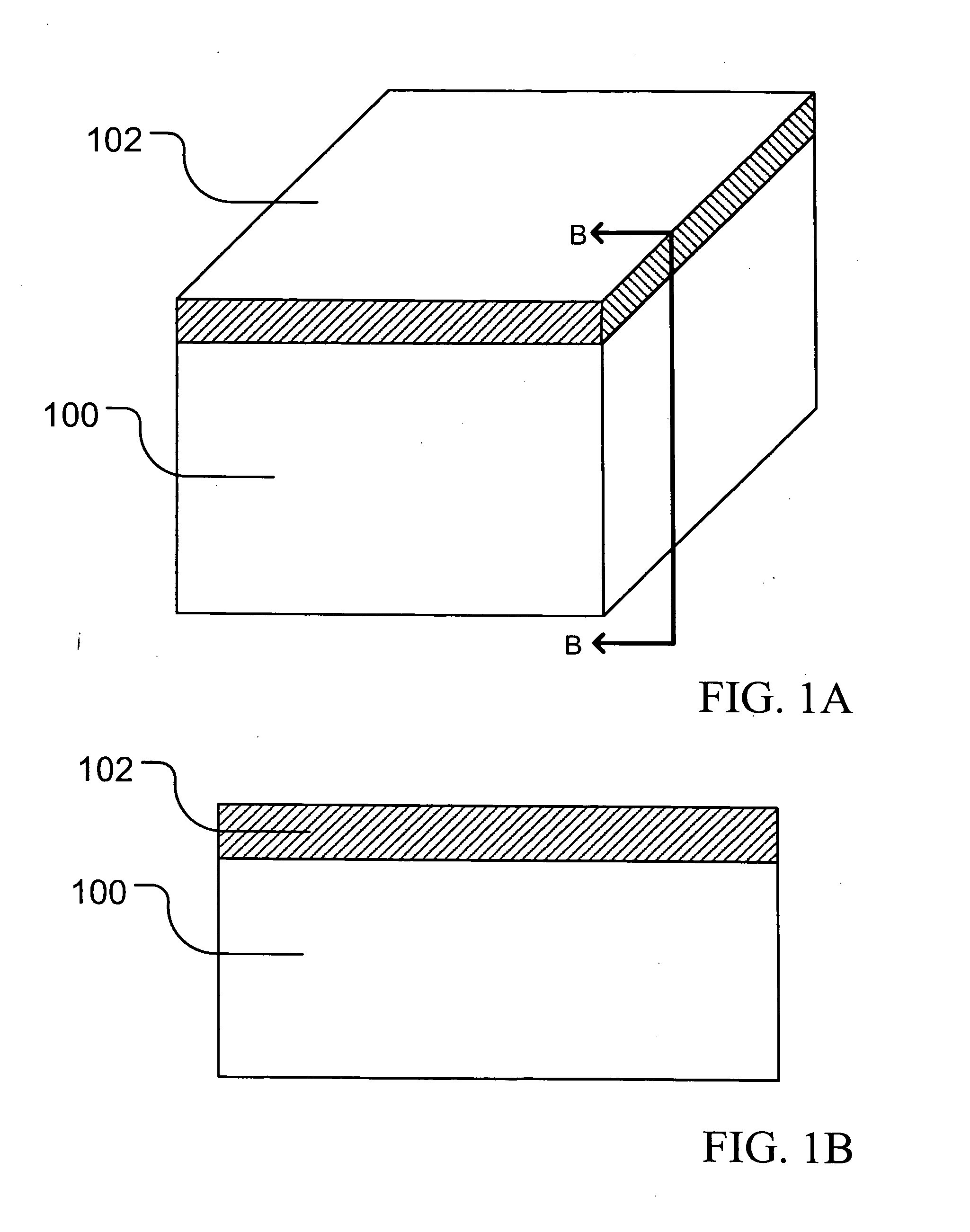
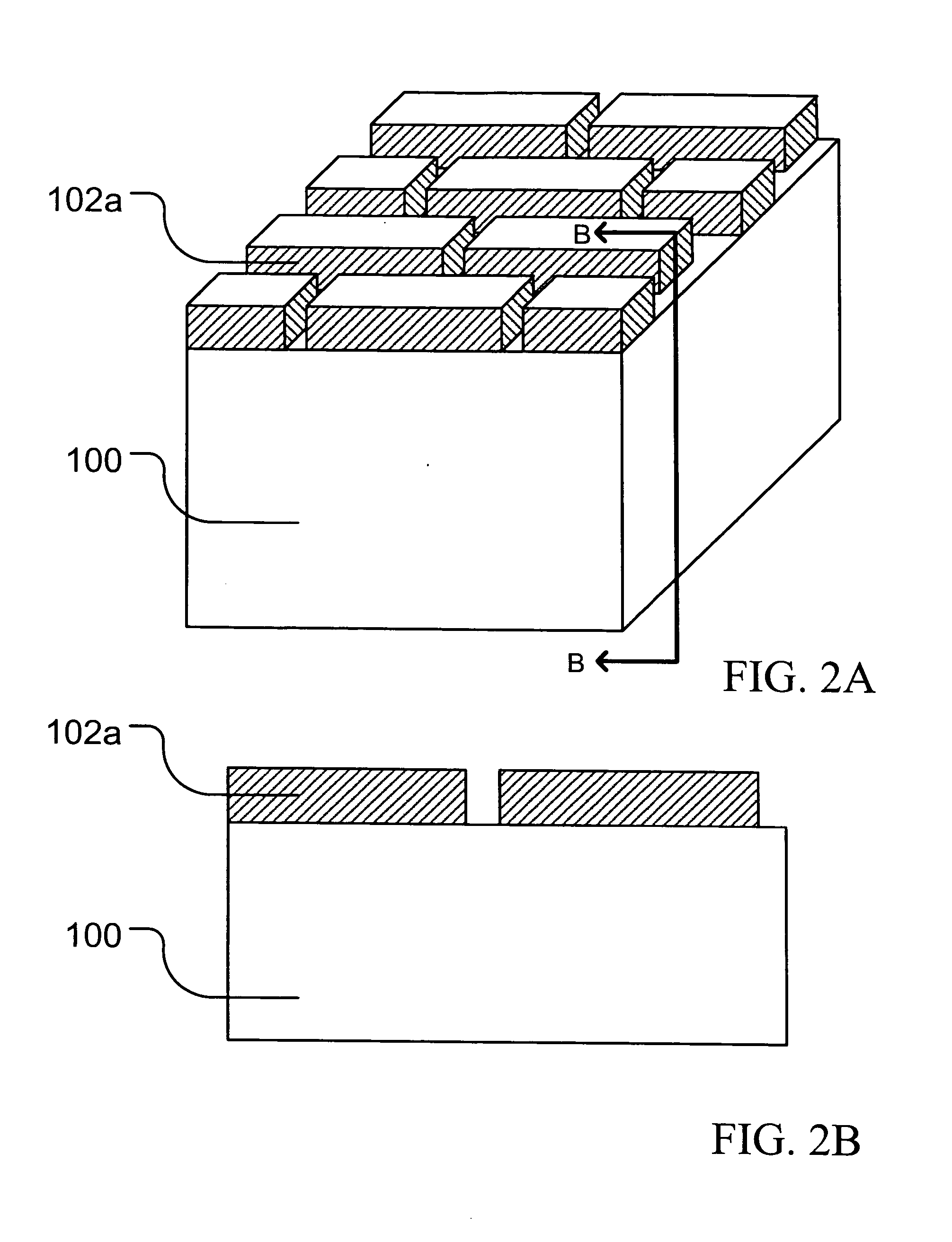
[0037] Hereinafter, example embodiments will be described more fully with reference to the accompanying drawings, in which example structures and process steps for fabricating such structures are shown. As will be appreciated by those skilled in the art, the associated figures are illustrative only and that other embodiments may take many different forms. The following claims, therefore, should not be construed as limited to the example embodiments. These example embodiments are provided so that this disclosure will be thorough and complete and thereby fully convey the concepts embodied by the examples to those skilled in the art. Indeed, other related embodiments may be and likely will be apparent to those of ordinary skill in the art based on the teachings provided in this disclosure in light of conventional knowledge in the art and are meant to be included to the extent consistent with the example embodiments detailed herein.

[0038] It will be understood that, although the terms ...


PUM


Abstract

Disclosed are methods for forming FinFETs using a first hard mask pattern to define active regions and a second hard mask to protect portions of the insulating regions between active regions. The resulting field insulating structure has three distinct regions distinguished by the vertical offset from a reference plane defined by the surface of the active regions. These three regions will include a lower surface found in the recessed openings resulting from the damascene etch, an intermediate surface and an upper surface on the remaining portions of the lateral field insulating regions. The general correspondence between the reference plane and the intermediate surface will tend to suppress or eliminate residual gate electrode materials from this region during formation of the gate electrodes, thereby improving the electrical isolation between adjacent active regions and improving the performance of the resulting semiconductor devices.

Description

PRIORITY STATEMENT [0001] This application claims priority under 35 U.S.C. § 119 from Korean Patent Application No. 10-2005-0108796, filed on Nov. 14, 2005, in the Korean Intellectual Property Office, the disclosure of which are hereby incorporated by reference in its entirety. BACKGROUND [0002] 1. Field of Endeavor[0003] The example embodiments relate to methods for manufacturing semiconductor devices, and more particularly, to methods for manufacturing semiconductor devices including fin-type channel regions. [0004] 2. Related Art [0005] As the integration density of semiconductor devices increases, the surface area available for forming conventional metal-oxide-semiconductor field effect transistor (MOSFET) is reduced correspondingly. For semiconductor devices utilizing conventional planar transistors, higher integration densities also lead to corresponding reductions in the channel lengths of the transistors utilized in such devices. The reduction in the channel lengths will ten...

Claims


Application Information

Patent Timeline
IPC IPC(8): H01L21/84H01L21/336
CPCH01L27/1211H01L29/66795H01L29/785H01L21/18
Inventor KIM, YONG-SUNGCHUNG, TAE-YOUNG
Owner SAMSUNG ELECTRONICS CO LTD
Why Eureka
Try Eureka