Vertical heterostructure field effect transistor and associated method

a heterostructure field and transistor technology, applied in the direction of basic electric elements, electrical apparatus, semiconductor devices, etc., can solve the problem that hfets are not effective in switching devices

Active Publication Date: 2007-05-24
GENERAL ELECTRIC CO
View PDF18 Cites 24 Cited by
  • Summary
  • Abstract
  • Description
  • Claims
  • Application Information

AI Technical Summary

Benefits of technology

[0006] In one embodiment, a normally-off electronic device is provided. The device may include a heterostructure field effect transistor. The transistor may include a first layer having a first material, and the first material having a hexagonal crystal lattice structure defining a first bandgap and one or more non-polar planes. The transistor may further include a second layer that is adjacent to the first layer having a second material. Further, the second layer has a first surface and a second surface, and a portion of the second layer first surface is coupled to the surface of the first layer to form a two dimensional charge gas and to define a first

Problems solved by technology

Therefore, such HFETs are not effective in swit

Method used


Image

  • Vertical heterostructure field effect transistor and associated method
  • Vertical heterostructure field effect transistor and associated method
  • Vertical heterostructure field effect transistor and associated method

Examples


example 1

Method of Forming a Normally-Off Heterostructure Field Effect Transistor

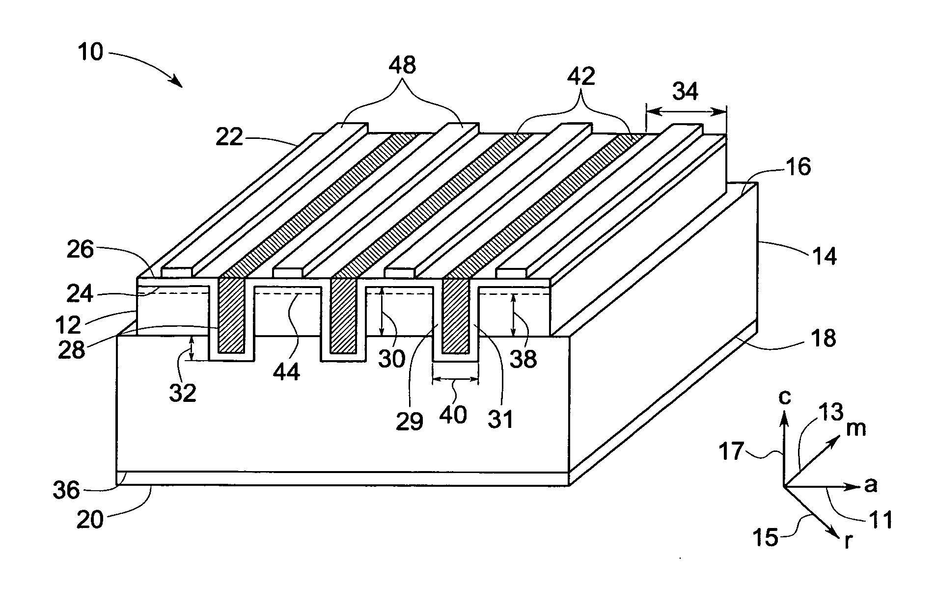
[0077] A lateral normally-off aluminum gallium nitride-gallium nitride heterostructure field effect transistor HFET is formed. In this structure, a 3 micrometers undoped a-plane gallium nitride epilayer is formed on a substrate. Subsequently, 25 nanometers Al0.3Ga.0.7N barrier layer is epitaxially grown on the a-plane gallium nitride layer. The aluminum gallium nitride layer includes a silicon delta-doped region which is located about 15 nanometers from the aluminum gallium nitride-gallium nitride interface. Next, a recess is etched in the aluminum gallium nitride layer to form a gate region approximately 10 nanometers deep, thus etching through the silicon delta-doped region in the aluminum gallium nitride layer. Next, metallization is done to deposit the conductive material of the gate. Subsequently, source and drain Ohmic contacts are formed. Since the aluminum gallium nitride-gallium nitride interface is on...

example 2

Method of Forming a Normally-Off Heterostructure Field Effect Transistor Employing a Dielectric Layer

[0078] A normally-off heterostructure field effect transistor is formed. The a-plane gallium nitride and aluminum gallium nitride layers are formed as described in the previous example. Subsequent to forming the recess for the gate electrode, a dielectric layer of 15 nanometers is formed on the aluminum gallium nitride layer by low-pressure chemical vapor deposition (LPCVD). This dielectric layer may be silicon dioxide. The metal gate electrode is formed on top of the dielectric. Next, the dielectric is etched away in the source and drain regions, and Ohmic contacts are formed to the source and drain. Using a dielectric between the gate electrode and the aluminum gallium nitride layer reduces gate leakage current during operation with positive gate-source bias voltages.

example 3

Method of Forming Normally-Off Heterostructure Field Effect Transistor Employing a Ion-Implanted Source and Drain Electrodes

[0079] In another embodiment, a lateral normally-off MOS-BFET is formed with Si-implanted source and drain contact regions. As in the previous embodiments, the a-plane gallium nitride and aluminum gallium nitride layers are formed by epitaxy. Next, the source and drain regions are ion-implanted using Silicon. Then, the aluminum gallium nitride surface is capped with a material such as aluminum nitride or silicon oxide and is annealed at 1400 degrees Celsius and 100 kilo bar at nitrogen overpressure for 30 minutes. The capping layer is then removed, and the surface is further processed as in the previous embodiment. The use of the silicon implanted source and drain regions provide a low resistance Ohmic contact to the channel layer.


PUM


Abstract

A vertical heterostructure field effect transistor including a first layer having a first material, and the first material having a hexagonal crystal lattice structure defining a first bandgap and one or more non-polar planes is provided. The transistor further includes a second layer that is adjacent to the first layer having a second material. Further, the second layer has a first surface and a second surface, and a portion of the second layer first surface is coupled to the surface of the first layer to form a two dimensional charge gas and to define a first region. The second material may have a second bandgap that is different than the first bandgap. Furthermore, the transistor may include a conductive layer that is disposed in the trench and is interposed between the first region and a second region that is not in electrical communication with the first region if no electrical potential is applied to the conductive layer, and an electrical potential applied to the conductive layer allows electrical communication from the first region to the second region.

Description

BACKGROUND [0001] The invention includes embodiments that may relate to a heterostructure field effect transistor. The invention includes embodiments that may relate to a method of making and / or using heterostructure field effect transistor. [0002] A field-effect transistor (FET) may be a transistor that relies on an electric field to control the conductivity of a “channel” in a semiconductor material. A FET, like all transistors, may be thought of as a voltage-controlled current source. Some FETs may use a single-crystal semiconductor wafer as the channel, or active region. A terminal in a FET may be one of a gate, a drain, or a source. The voltage applied between gate and source terminals may modulate the current between the source and the drain. [0003] A HFET is a heterostructure field effect transistor, and may be called a HEMT for High Electron Mobility Transistor. A HEET or a HEMT may be a field effect transistor with a junction between two materials with different band gaps (...

Claims


Application Information

Patent Timeline
IPC IPC(8): H01L31/00
CPCH01L29/045H01L29/2003H01L29/42316H01L29/4236H01L29/7787H01L29/7788H01L29/7789
Inventor MATOCHA, KEVIN SEANTILAK, VINAYAK
Owner GENERAL ELECTRIC CO
Why Eureka
Try Eureka