Conductor track arrangement and associated production method

a technology of conductor track and production method, which is applied in the direction of semiconductor/solid-state device details, electrical apparatus, semiconductor devices, etc., can solve the problems of increased signal delay, power dissipation and crosstalk in the semiconductor chip, and high cost of known production methods, so as to achieve high quality, reduce costs, and simplify production methods

Inactive Publication Date: 2007-05-31
INFINEON TECH AG
View PDF14 Cites 25 Cited by
  • Summary
  • Abstract
  • Description
  • Claims
  • Application Information

AI Technical Summary

Benefits of technology

[0012] An insulating layer is preferably formed on the surface of the conductor tracks, on the surface of the carrier tracks and on the surface of the substrate or on the surface of the carrier layer, respectively, toward the cavity, as a result of which short circuits between adjacent conductor tracks, caused by electromigration, can be considerably reduced. In this context, on the one hand, this insulating layer covering the exposed surfaces of the conductor track at least impedes an out-diffusion of conductor track material in the cavity, occurring due to electromigration processes. In particular, however, such an insulating layer prevents a short circuit between adjacent conductor tracks caused by this process.
[0013] This insulating layer is preferably formed in one piece with a resist layer which covers the conductor tracks and closes off or seals the cavity. This further simplifies the production method and reduces costs.
[0014] The production method performed is, in particular, a non-conformal CVD deposition process with SiH4 and N2O in the ratio of SiH4:N2O=1:5 to 1:20 at a pressure of 1 to 10 torr (133 to 1333 Pa), a temperature of 350 to 450 degrees Celsius and an RF power of 200 to 400 watts. With this special deposition process and the associated parameters, the insulating layer described above can be formed with high quality on all exposed surfaces of the conductor tracks whereas the cavities between the conductor tracks are covered or sealed toward the top at the same time. This further reduces production costs with improved electric characteristics.
[0015] The substrate can preferably also precisely specify an etch barrier for determining a depth of the undercut part-cavity which allows the process to be better controlled. As an alternative, however, a corresponding predetermined etch depth can be set even without such an etch barrier but by monitoring a predetermined etching time. In this manner, a conductor track arrangement with self-aligning support structures can be produced cost-effectively without using additional lithographic steps and with good mechanical stability.

Problems solved by technology

Apart from the aforementioned increase in capacitances between the conductor tracks, this also leads to an increase in signal delays, power dissipation and crosstalk in the semiconductor chip.
The disadvantageous factor, however, is that the known production methods are extremely complex and thus cost-intensive, and the completed conductor track arrangement has poor mechanical stability.
Furthermore, the reduction in coupling capacitances is not optimal.

Method used


Image

  • Conductor track arrangement and associated production method
  • Conductor track arrangement and associated production method
  • Conductor track arrangement and associated production method

Examples


Embodiment Construction

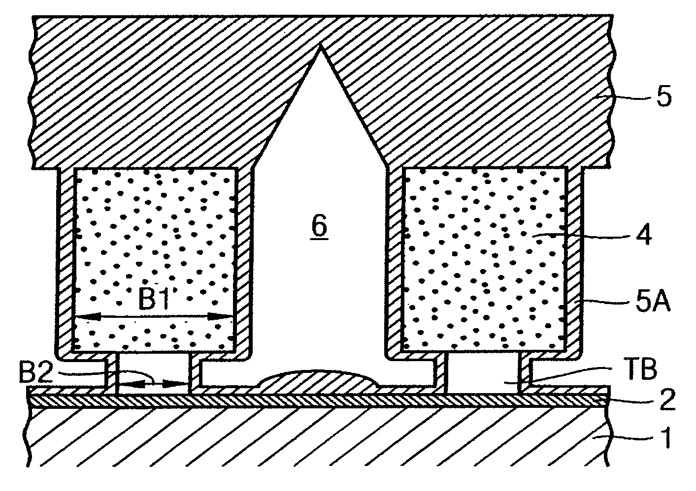
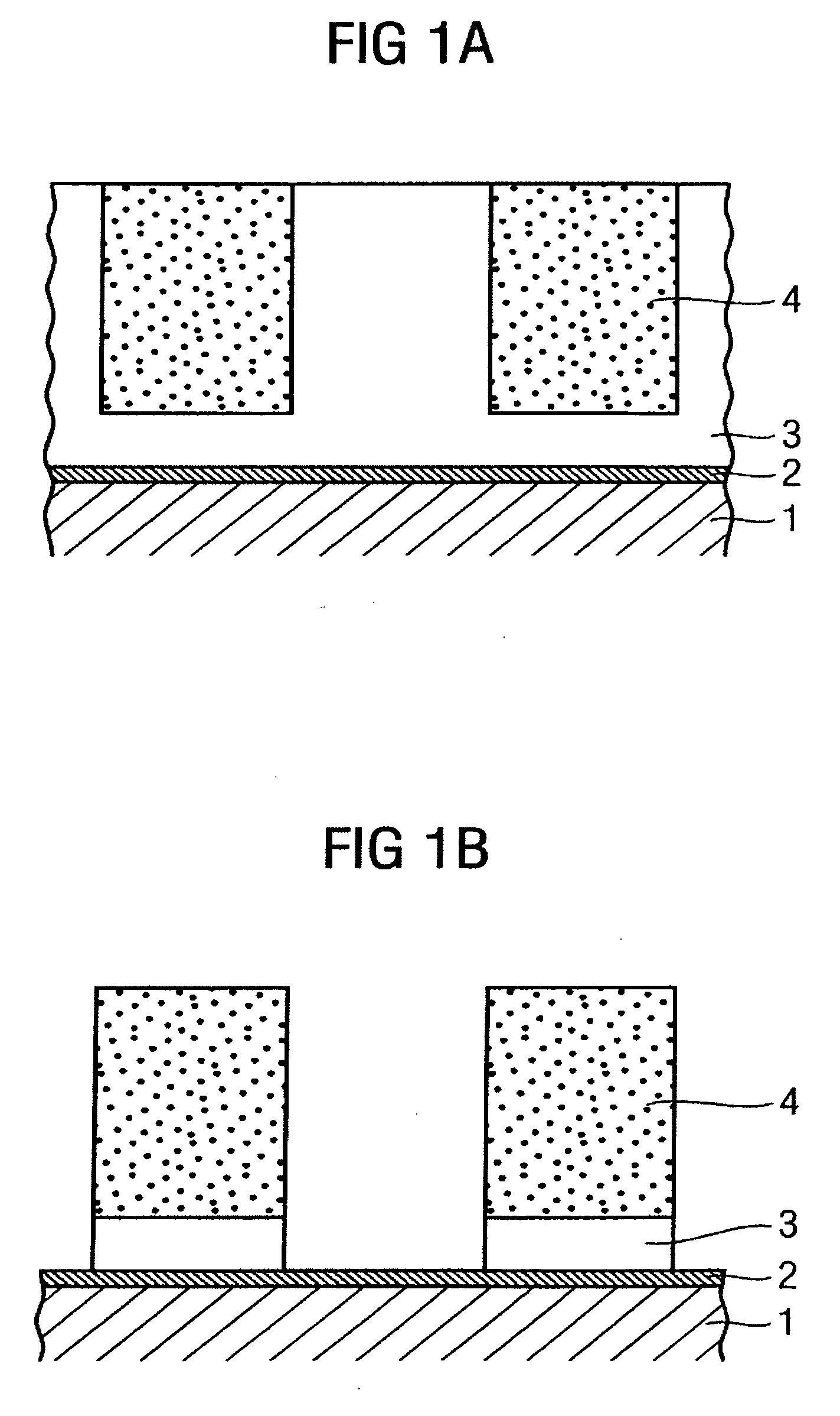
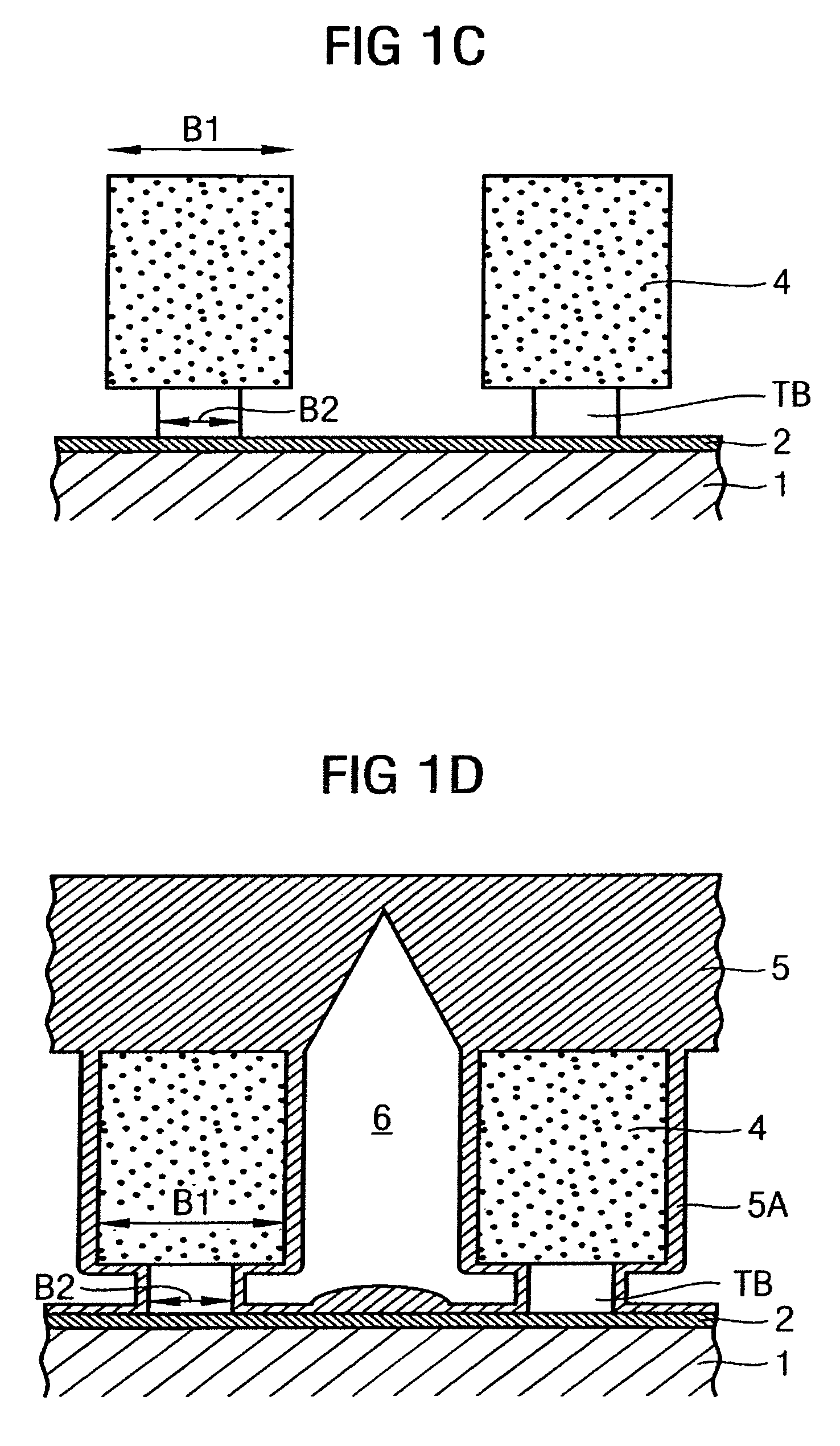
[0020]FIGS. 1A to 1D show sectional views for illustrating steps during the production of a conductor track arrangement according to a first exemplary embodiment, performing a “damascene process” for forming the conductor tracks.

[0021] The disclosure shows a first metallization level, i.e., a lowermost conductor track level which is located in the immediate vicinity of the semiconductor substrate, not shown, since the extent of the cavities according to the disclosure laterally underneath the conductor tracks, in particular, leads to a reduction of the coupling capacitances of the conductor tracks to a semiconductor substrate lying underneath or to conductor tracks lying underneath.

[0022] According to FIG. 1A, a conductor track pattern of conductor tracks 4 is formed by a damascene process in a dielectric substrate. The substrate according to the first exemplary embodiment can have a first dielectric or a first dielectric layer 1, an etch barrier 2 formed thereon and a second diel...


PUM


Abstract

A conductor track arrangement includes a substrate, at least two conductor tracks, a cavity and a resist layer that covers the conductor tracks and closes off the cavity. By forming carrier tracks with a width less than a width of the conductor tracks, air gaps can also be formed laterally underneath the conductor tracks for reducing the coupling capacitances and the signal delays in a self-aligning manner.

Description

PRIORITY CLAIM [0001] The present application claims the benefit of priority of German Patent Application No. DE 10 2005 039 323.3, filed Aug. 19, 2005, the contents of which are incorporated by reference herein. TECHNICAL FIELD [0002] The present invention relates to a conductor track arrangement and an associated production method and, in particular, to a conductor track arrangement with cavities or so-called “air gaps.”BACKGROUND [0003] Conductor track arrangements are used, in particular, in semiconductor technology for implementing the wiring of semiconductor components. In this arrangement, a dielectric layer or insulating layer is usually formed on an electrically conductive carrier substrate such as, for example, a semiconductor substrate, and on this an electrically conductive conductor track layer is formed, the conductor track layer, after patterning, representing the final conductor track. Following that, further insulating layers and electrically conductive layers are f...

Claims


Application Information

Patent Timeline
Patent Type & Authority Applications(United States)
IPC IPC(8): H01L23/48
CPCH01L21/7682
Inventor GABRIC, ZVONIMIRPAMLER, WERNERSCHINDLER, GUENTHERSTICH, ANDREAS
Owner INFINEON TECH AG
Why Eureka
Try Eureka