Metal oxide semiconductor film structures and methods

a metal oxide and semiconductor film technology, applied in the field of semiconductors, can solve the problems of significant affecting device sensitivity, response time, read-out noise, and limited use of znmgo alloys

Inactive Publication Date: 2007-06-07
MOXTRONICS
View PDF7 Cites 57 Cited by
  • Summary
  • Abstract
  • Description
  • Claims
  • Application Information

AI Technical Summary

Benefits of technology

[0025] The atomic fraction y of Cd and the atomic fraction z of Se in the ZnCdOSe alloy system, namely, Zn1-yCdyO1-zSez, can be varied to decrease the energy band gap of ZnO to values smaller than that of ZnO.

Problems solved by technology

These effects significantly affect device sensitivity, response time, and read-out noise.
Therefore, ZnMgO alloys are limited in use for increasing the energy band gap in semiconductor devices up to 3.3 eV but not to larger energy band gap values.

Method used


Image

  • Metal oxide semiconductor film structures and methods
  • Metal oxide semiconductor film structures and methods
  • Metal oxide semiconductor film structures and methods

Examples


examples and embodiments

OF THE INVENTION

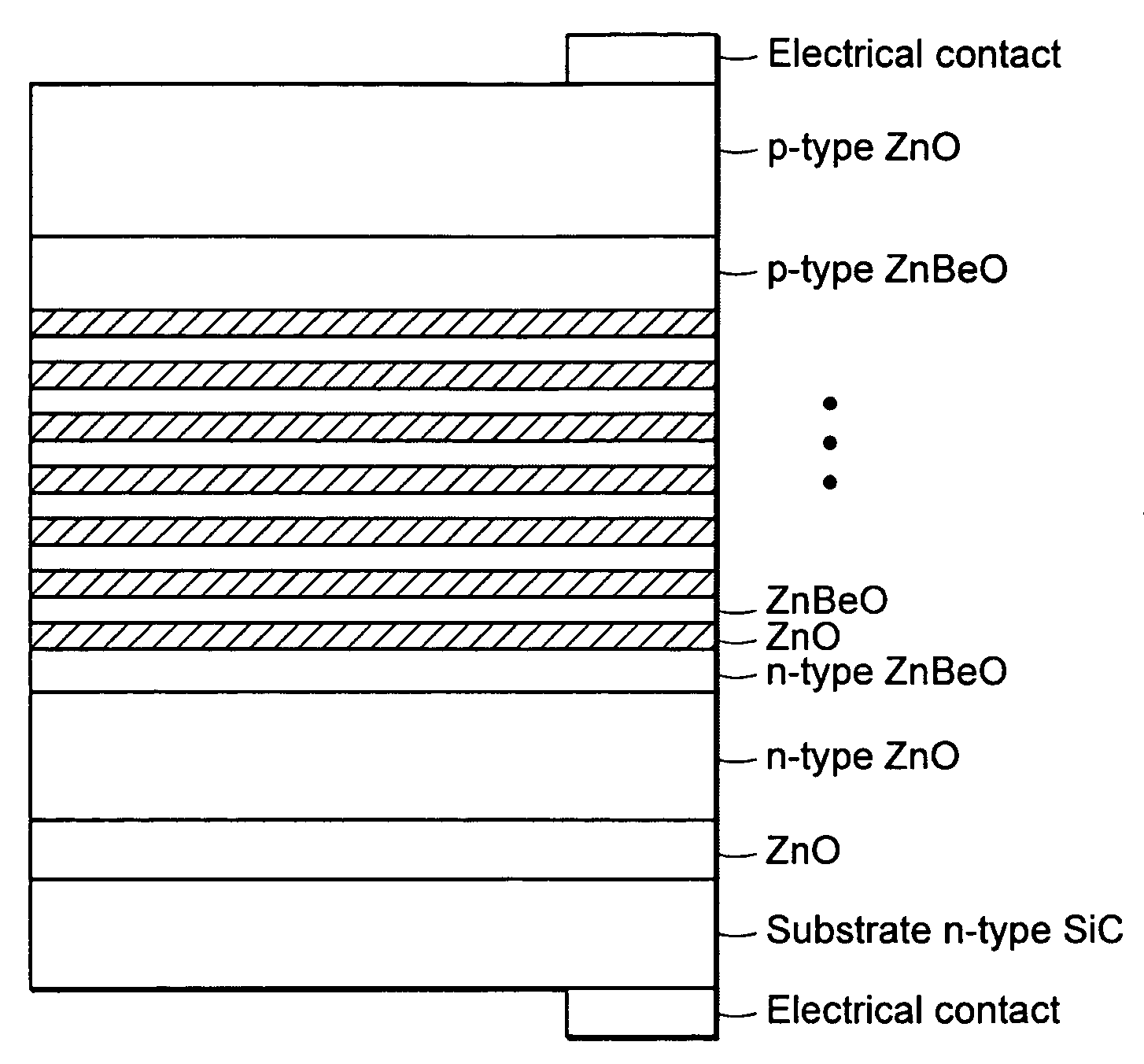
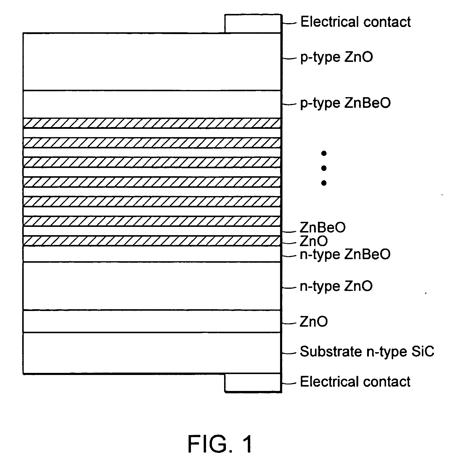
[0068] MQW: A first embodiment of the present invention is a ZnO based semiconductor LED device with a structure as shown in FIG. 1. The LED device in FIG. 1 has a MQW structure comprised of alternating layers of ZnO and ZnBeO semiconductor layers with the MQW active layer region formed between confinement and cladding layers, with semiconductor layers laminated successively on a n-type SiC substrate. In one example the thickness of each of the ZnO layers in the active layer region was about 3 nm, the thickness of each of the ZnBeO layers in the active layer region was about 5 nm, each of the ZnO semiconductor active layers in the active layer region was undoped, and each of the ZnBeO semiconductor well boundary layers in the active layer region was undoped.

[0069] In other such examples, a ZnO semiconductor active layer may be doped or undoped, and may contain also one or more of the elements Si, Se, Cd and Ba; and a ZnBeO semiconductor well boundary layer may be do...


PUM


Abstract

Layered and film structures for improving the performance of semiconductor devices include single and multiple quantum wells and double heterostructures and superlattice structures.

Description

FIELD OF THE INVENTION [0001] The present invention relates generally to semiconductors, and, more particularly, to zinc oxide based and other metal oxide and metal oxide alloy based semiconductor devices and film structures. BACKGROUND OF THE INVENTION [0002] The optical properties of zinc oxide (ZnO) have been studied for potential use in semiconductor devices, in particular for photonic light emitting devices such as light emitting diodes (LEDs) and laser diodes (LDs) and photonic detectors such as photodiodes. The energy band gap of ZnO is approximately 3.3 electron volt (eV) at room temperature, corresponding to a wavelength of approximately 376 nanometer (nm) for an emitted photon of this energy. Light emission has been demonstrated from ZnO LEDs using p-type and n-type materials to form a diode. ZnO has also been used to fabricate a UV photodetector and a field effect transistor (FET). [0003] ZnO has several important properties that make it a promising semiconductor material...

Claims


Application Information

Patent Timeline
Patent Type & Authority Applications(United States)
IPC IPC(8): H01L33/00H01L33/06H01L33/28
CPCB82Y20/00H01L33/06H01L33/28H01S5/327H01S5/34H01S5/3425
Inventor RYU, YUNGRYELLEE, TAE-SEOKWHITE, HENRY W.
Owner MOXTRONICS
Why Eureka
Try Eureka