Capacitor and method of manufacturing same

a technology of capacitors and dielectric layers, applied in the field of capacitors, can solve the problems of increasing reducing the withstand voltage in some cases, short-circuit failure and/or an increase in the leakage current of the dielectric layer, so as to prevent an increase in the leakage current

Active Publication Date: 2007-06-14
TDK CORPARATION
View PDF10 Cites 12 Cited by
  • Summary
  • Abstract
  • Description
  • Claims
  • Application Information

AI Technical Summary

Benefits of technology

[0012] It is a first object of the invention to provide a capacitor comprising a lower electrode made of a foil, an upper electrode layer, and a dielectric layer disposed between the lower electrode and the upper electrode layer, the capacitor being capable of preventing an increase in leakage current of the dielectric layer and an occurrence of short-circuit failure that are not caused by defects of the dielectric layer, and to provide a method of manufacturing such a capacitor.
[0013] It is a second object of the invention to provide a method of manufacturing a capacitor comprising a lower electrode, an upper electrode layer, and a dielectric layer disposed between the lower electrode and the upper electrode layer, the method being capable of preventing an increase in leakage current of the dielectric layer and an occurrence of short-circuit failure while suppressing degradation of characteristics of the capacitor.
[0023] According to the capacitor or the first method of manufacturing the capacitor of the invention, the resin insulator is disposed between the top surface of the dielectric layer and the bottom surface of the upper electrode layer and is present only in part of the region in which the top surface of the dielectric layer and the bottom surface of the upper electrode layer face each other. The resin insulator is disposed to cover at least part of the grain boundaries appearing at the top surface of the lower electrode when seen from above the top surface of the dielectric layer. As a result, according to the invention, it is possible to prevent an increase in leakage current of the dielectric layer and an occurrence of short-circuit failure that are caused by the grain boundaries appearing at the top surface of the lower electrode.
[0024] According to the second method of manufacturing a capacitor of the invention, in the step of forming the resin insulator for repairing the defect of the dielectric layer, a step of forming by electrophoresis an electro-deposit that will be part of the resin insulator later and a step of increasing the electrical resistance of the electro-deposit are alternately repeated a plurality of times. As a result, according to the invention, it is possible to form the resin insulator in a small thickness and to thereby prevent an increase in leakage current of the dielectric layer and an occurrence of short-circuit failure while suppressing degradation of characteristics of the capacitor.
[0025] According to the third method of manufacturing a capacitor of the invention, it is possible not only to prevent an increase in leakage current of the dielectric layer and an occurrence of short-circuit failure that result from defects of the dielectric layer but also to prevent an increase in leakage current and an occurrence of short-circuit failure of the dielectric layer that result from the lower electrode formed of a foil made of a polycrystalline metal.

Problems solved by technology

As disclosed in this publication, conventional thin-film capacitors have a problem that, if the thickness of the dielectric layer is reduced, leakage current of the dielectric layer is increased and / or the withstand voltage of the dielectric layer is reduced.
However, in the thin-film capacitors manufactured by stacking the dielectric layer and the upper electrode layer on the metallic foil through thin-film forming techniques as described above, a short-circuit failure and / or an increase in leakage current of the dielectric layer has been found to occur in some cases even if the dielectric layer has no defect.
As disclosed in Japanese Published Patent Application 2002-26266, it is known that an increase in leakage current of the dielectric layer and a reduction in withstand voltage of the dielectric layer can occur due to defects existing in the dielectric layer.
In a case in which an insulator is provided on or below a part of the dielectric layer in a thin-film capacitor to prevent the occurrence of short-circuit failure and an increase in leakage current of the dielectric layer, if the insulator is too large, the characteristics of the capacitor may be degraded due to the existence of the insulator.

Method used


Image

  • Capacitor and method of manufacturing same
  • Capacitor and method of manufacturing same
  • Capacitor and method of manufacturing same

Examples


first embodiment

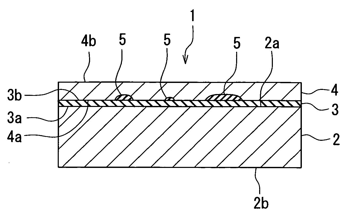
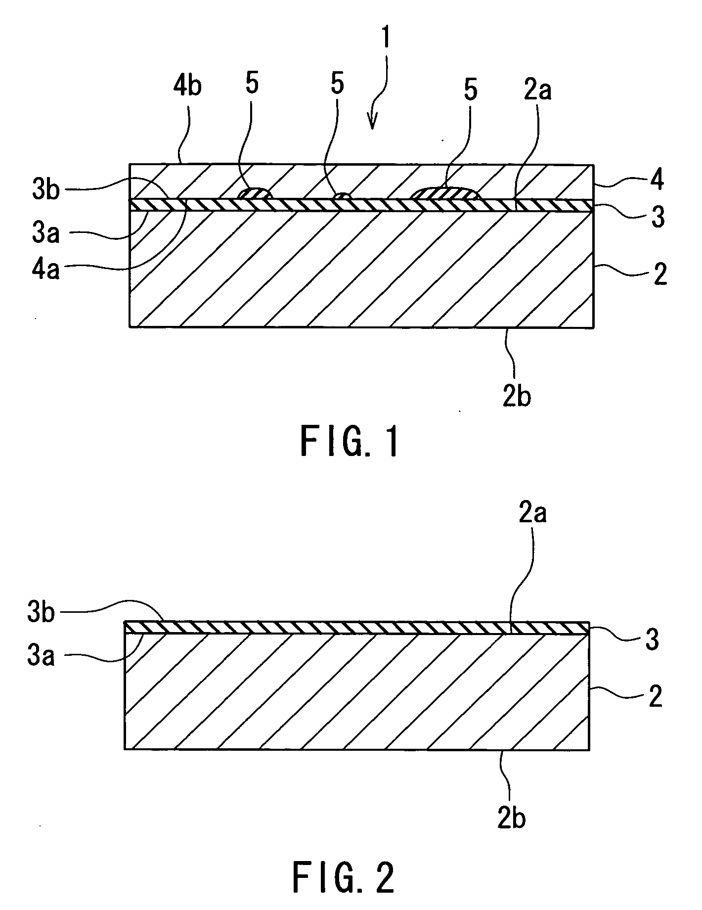
[0043] Preferred embodiments of the invention will now be described in detail with reference to the accompanying drawings. Reference is now made to FIG. 1 to describe the configuration of a capacitor of a first embodiment of the invention. FIG. 1 is a cross-sectional view of the capacitor of the embodiment. As shown in FIG. 1, the capacitor 1 of the embodiment comprises: a lower electrode 2 formed of a foil made of a polycrystalline metal; an upper electrode layer 4; and a dielectric layer 3 disposed between the lower electrode 2 and the upper electrode layer 4.

[0044] The lower electrode 2 has a top surface 2a facing the dielectric layer 3, and a bottom surface 2b opposite to the top surface 2a. Since the lower electrode 2 is polycrystalline, it is made up of a number of crystals, which is different from an amorphous structure, and there appear crystal grain boundaries at the top surface 2a. The crystal grain diameter is around 1 to 500 μm when evaluated by converting the shape of ...

second embodiment

[0088] A method of manufacturing a capacitor of a second embodiment of the invention will now be described. Reference is first made to FIG. 8 to describe the configuration of the capacitor manufactured through the method of the second embodiment. FIG. 8 is a cross-sectional view illustrating a portion of the capacitor. As shown in FIG. 8, the capacitor 1 of the embodiment comprises: the lower electrode 2, the upper electrode layer 4, and the dielectric layer 3 disposed between the lower electrode 2 and the upper electrode layer 4.

[0089] The lower electrode 2 is formed of a foil made of a polycrystalline metal, for example. In this case, the lower electrode 2 has a configuration the same as that of the first embodiment. The upper electrode layer 4 of the second embodiment has a configuration the same as that of the first embodiment, too. The dielectric layer 3 of the second embodiment has a defect 31 such as a pinhole. The remainder of configuration of the dielectric layer 3 is the ...

first example

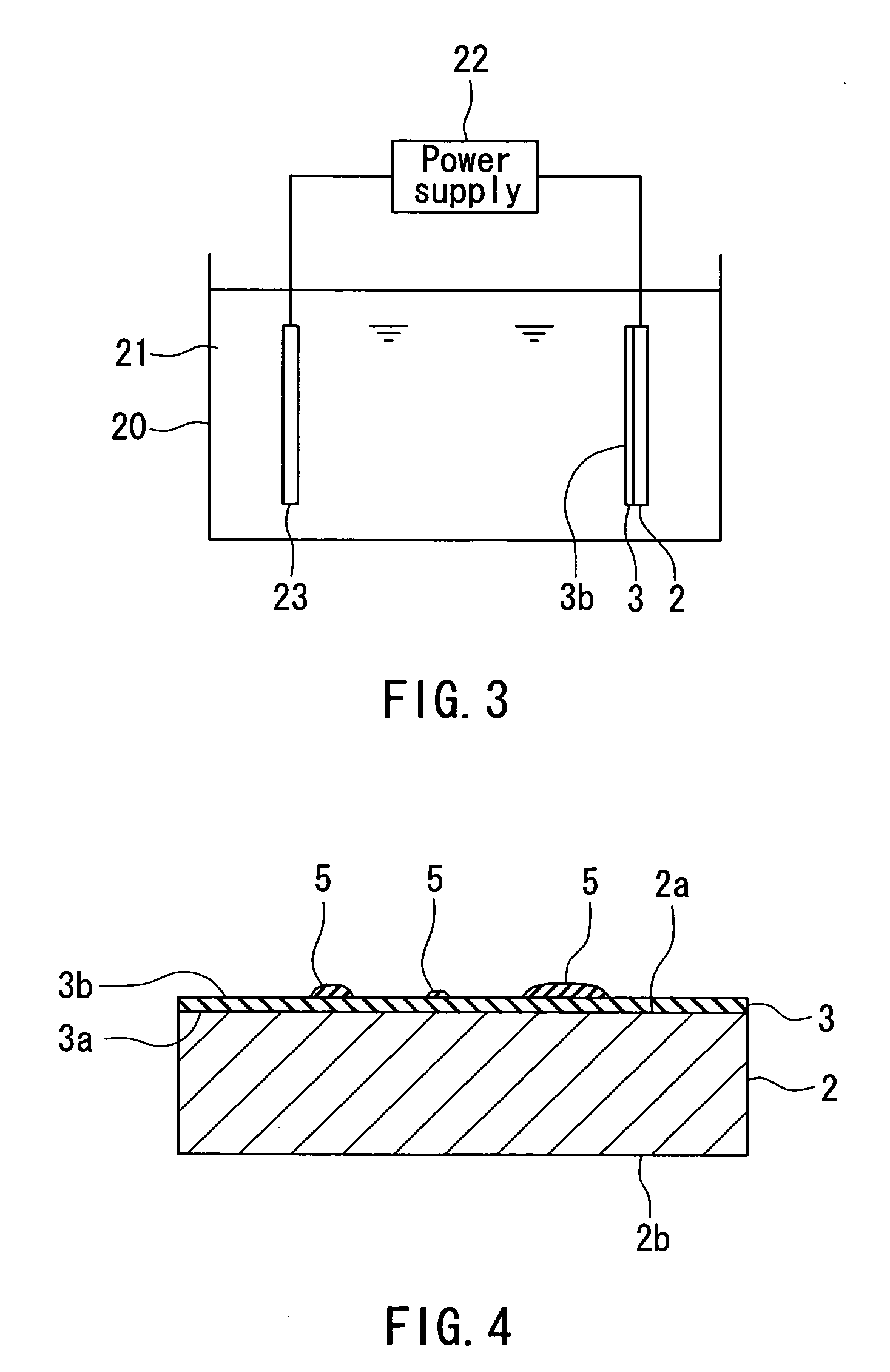
[0112] In a first example, the electrodeposition step and the resistance raising step are alternately repeated twice in the step of forming the resin insulator 5. In the first resistance raising step, the electro-deposit 51 is dried. In the second resistance raising step, the electro-deposit 52 is dried and then the electro-deposits 51 and 52 are cured by heating.

[0113] In the first example, first, an electrolytic nickel foil having a thickness of 30 μm was subjected to heat treatment at a temperature of 1000° C. in a nitrogen atmosphere, and then buffing was performed to flatten the surface. This nickel foil was used as the lower electrode 2. As a result of analyzing the content of impurities listed in the table 1 on the electrolytic nickel foil used as the lower electrode 2, the total impurities content was 310 ppm. Next, the dielectric layer 3 made of barium titanate having a thickness of 200 nm was formed by MOD on the top surface 2a of the lower electrode 2. To be specific, a ...


PUM

PropertyMeasurementUnit
grain diameteraaaaaaaaaa
thicknessaaaaaaaaaa
thicknessaaaaaaaaaa

Abstract

A capacitor comprises: a lower electrode formed of a foil made of a polycrystalline metal; an upper conductor layer; and a dielectric layer disposed between the lower electrode and the upper electrode layer. Grain boundaries of the polycrystalline metal appear at the top surface of the lower electrode. The capacitor further comprises an insulator that is disposed between the top surface of the dielectric layer and the bottom surface of the upper electrode layer and that is present only in part of a region in which the top surface of the dielectric layer and the bottom surface of the upper electrode layer face each other. The insulator is disposed to cover at least part of the grain boundaries appearing at the top surface of the lower electrode when seen from above the top surface of the dielectric layer. The insulator is formed by electrophoresis.

Description

BACKGROUND OF THE INVENTION [0001] 1. Field of the Invention [0002] The present invention relates to a capacitor comprising a lower electrode, an upper electrode layer, and a dielectric layer disposed between the lower electrode and the upper electrode layer, and to a method of manufacturing such a capacitor. [0003] 2. Description of the Related Art [0004] With increasing demands for reductions in dimensions and thickness of high frequency electronic apparatuses such as cellular phones, reductions in dimensions and height of electronic components mounted on the high frequency electronic apparatuses have been sought. One of the electronic components is a capacitor. The capacitor typically incorporates a dielectric layer and a pair of electrode layers disposed to sandwich the dielectric layer. [0005] To achieve reductions in dimensions and height of a capacitor, important factors are a reduction in area of a region in which the pair of electrode layers are opposed to each other with t...

Claims


Application Information

Patent Timeline
Patent Type & Authority Applications(United States)
IPC IPC(8): H01L27/108
CPCH01G4/206H01L28/55H05K1/162H05K2201/0175H05K2201/0195H05K2201/0355H05K2201/09309H05K2203/1105H05K2203/135
Inventor OZAKI, YUMIKOSHINOURA, OSAMU
Owner TDK CORPARATION
Why Eureka
Try Eureka