Hot melt adhesive composition

a technology of adhesive composition and hot melt, which is applied in the direction of polyether adhesives, non-macromolecular adhesive additives, film/foil adhesives, etc., can solve the problems of low heat resistance, low dispersion accuracy, and prone to breakage of wafers or devices, and achieves easy peeling of semiconductor wafers, easy cleaning or removal, and thin grinding

Inactive Publication Date: 2007-06-14
JSR CORPORATIOON
View PDF5 Cites 4 Cited by
  • Summary
  • Abstract
  • Description
  • Claims
  • Application Information

AI Technical Summary

Benefits of technology

[0013] According to the present invention, there is provided a hot-melt adhesive composition which is capable of firmly fixing a semiconductor wafer or the like onto a substrate when heated to molten and cooled and which enables easy peeling of the semiconductor wafer or the like from the substrate when heated to molten again.
[0014] In the case where the hot-melt adhesive composition of the invention is used, the adhesive component remaining on the surface of the wafer or the like after the wafer or the like is peeled from the substrate can be easily cleaned or removed.
[0015] Because of the above properties, the hot-melt adhesive composition of the invention can be favorably used as an adhesive for temporarily bonding a substrate in various processing stages necessary in scenes of the economical activities of the present day, for example, extremely thin grinding of semiconductor substrate and fine processing of surfaces of various materials.

Problems solved by technology

Such conventional waxes, however, have low heat resistance, so that there are various problems.
For example, the bond strength cannot be retained at the processing temperature in the wafer grinding step, the in-plane dispersion accuracy of the thickness of the ground wafer is not satisfactory, when a thin-ground semiconductor wafer or semiconductor device is peeled, the wafer or the device is liable to be broken because of bad releasability, if bubbles remain on the bonded surface, irregularities are produced on the back surface of the wafer, and if grinding is carried out in this state, the wafer is liable to be broken.

Method used


Image

  • Hot melt adhesive composition
  • Hot melt adhesive composition
  • Hot melt adhesive composition

Examples


example 1

[0076] Into a cylindrical pressure molding machine having a diameter of 10 mm, 0.354 g of cholesterol (molecular weight: 386.7, melting temperature: 150° C., melting temperature width: 1° C., melt viscosity: 2 mPa·s) was weighed, and a pressure of 200 kg·cm−2 was applied for 3 minutes to obtain a cylindrical tablet having a diameter of 10 mm and a thickness of 5.5 mm.

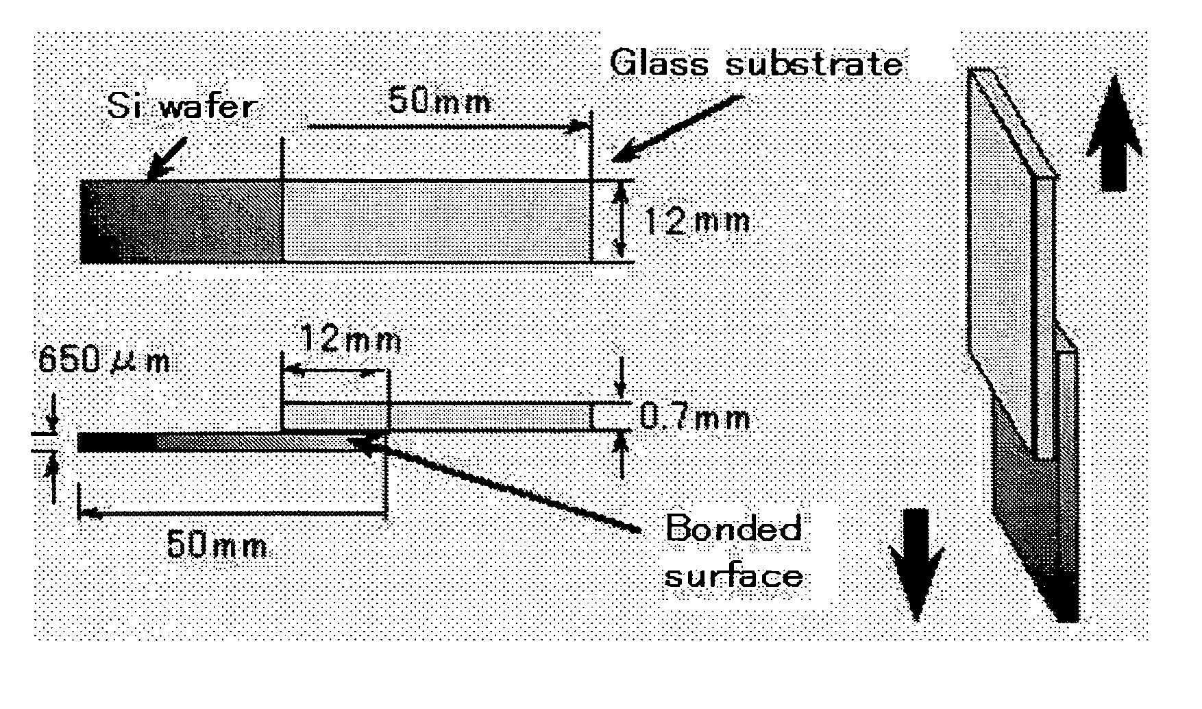
[0077] The resulting tablet was placed on a 6-inch silicon wafer (thickness: 650 mm), then a square glass substrate having a thickness of 0.7 mm and a side length of 20 cm was placed on the tablet, and they were placed in a vacuum oven and heated to 150° C. at 10 Torr. As the 6-inch silicon wafer to be bonded, a wafer whose surface had been subjected to hydrophobicity-imparting treatment consisting of spin coating with a 5% isopropyl alcohol solution of hexamethyldisilazane and drying was used. The tablet was melted at a wafer temperature of about 148° C. At this time, vacuum drawing was terminated, and the cholesterol...

example 2

[0080] An aluminum substrate was laminated onto a glass substrate in the same manner as in Example 1, except that a 6-inch aluminum substrate (thickness: 3 mm) whose surface to be laminated had been partially provided with a fine wiring pattern of 10 μmL / S and 5 μm depth was used instead of the 6-inch silicon wafer, a mixture (melting temperature: 157° C., melting temperature width: 1° C., melt viscosity: 1 mPa·s) of 0.5 g of ergosterol (molecular weight: 396.7, melting point: 157° C.), 0.05 g of a surface active agent “SF-8428” (available from Dow Corning Toray Silicon Co., Ltd.) and 0.03 g of silicon dioxide fine particles (available from Shionogi & Co., Ltd., mean particle diameter: 2 μm) was used instead of cholesterol, and the heating temperature of the vacuum oven was changed to 160° C. The bond strength was 4.6 MPa (25° C.), and a difference between the bond strength at 25° C. and the bond strength at 137° C. was 0.2 MPa. The tensile shear strength of the sample (laminate of ...

example 3

[0083] A copper foil (roughened side) was laminated onto a glass substrate in the same manner as in Example 1, except that a square electrodeposited copper foil (thickness: 25 μm) having a side length of 13 cm was used instead of the 6-inch silicon wafer. Then, the shiny side of the copper foil was coated with an insulating film varnish “WPR-1020” (available from JSR Corporation) in a thickness of 2 μm by spin coating, and the varnish was dried at 140° C. for 1 hour to form an insulating film. A dispersion of the thickness of the insulating film was measured. As a result, a mean film thickness was 2.05 μm, and the dispersion was 0.02 μm. This dispersion was equivalent to that in the case of formation of an insulating film on a usual silicon wafer by spin coating, and it was found that lamination between the glass substrate and the copper foil had been uniformly carried out. Further, even in the drying step at 140° C. to form an insulating film, the copper foil did not peel off from ...


PUM

PropertyMeasurementUnit
melt viscosityaaaaaaaaaa
melting temperatureaaaaaaaaaa

Abstract

[Problem] To provide an adhesive composition which is used for fixing a semiconductor wafer or the like onto a substrate, exhibits firm adhesion with high heat resistance in the wafer grinding stage and is melted by heating to enable easy peeling after the completion of the wafer grinding stage. [Means to solve problem] The hot-melt adhesive composition of the invention is a composition containing as a main component a crystalline compound having a melting temperature of 50 to 300° C., and has a melting temperature width of not more than 30° C. and a melt viscosity of not more than 0.1 Pa·s. The crystalline compound as a main component is desired to be an organic compound composed of elements of C, H and O only and having a molecular weight of not more than 1000, preferably an aliphatic compound or an alicyclic compound, particularly preferably a compound having a steroid skeleton and / or a hydroxyl group.

Description

TECHNICAL FIELD [0001] The present invention relates to an adhesive composition used for fixing a semiconductor wafer onto a substrate in the processing of the wafer. More particularly, the invention relates to an adhesive composition which exhibits satisfactory adhesion at a processing temperature in the wafer processing stage, enables easy peeling of the wafer from the substrate after the processing of the wafer and can be easily removed when it has stuck and remain on the wafer after the processing. BACKGROUND ART [0002] In the manufacturing process of semiconductor devices, a great number of lattice-like circuits such as IC and LSI are formed on a surface of a semiconductor wafer that is in a substantially disc form, and each region where the circuit has been formed is subjected to dicing along the given cutting lines to manufacture an individual semiconductor device. In the manufacture of the semiconductor device in this manner, it is desirable to make the thickness of the semi...

Claims


Application Information

Patent Timeline
Patent Type & Authority Applications(United States)
IPC IPC(8): C09J7/02C09J11/06C09J201/00H01L21/68
CPCC09J11/06C08K5/05C09J11/00C09J11/08C09J171/00C09J201/00
Inventor YASUDA, KYOUYUITOU, NOBUYUKIYOKOYAMA, YASUAKIYOKOYAMA, MICHIKO
Owner JSR CORPORATIOON
Why Eureka
Try Eureka