Silicon carbide semiconductor device and method for producing the same

Inactive Publication Date: 2007-06-21
NISSAN MOTOR CO LTD +1
View PDF4 Cites 39 Cited by
  • Summary
  • Abstract
  • Description
  • Claims
  • Application Information

AI Technical Summary

Benefits of technology

[0011] According to a fourth aspect of the present invention, there is provided a method for producing a silicon carbide semiconductor device which comprises: 1) a silicon carbide substrate; 2) a silicide electrode configured to be formed by depositing a contact parent material on the silicon carbide substrate in such a manner as to cause a solid phase reaction, the silicide electrode being a lower carbon content silicide electrode including: i) silicon, and ii) carbon smaller than the silicon in mol number; and 3) an upper conductor film deposited to the silicide electrode, wherein the silicon carbide semiconductor device further comprises: 1) a source electrode including the lower carbon content silicide electrode, and 2) a drain electrode including the lower carbon content silicide electrode, allowing the silicon carbide semiconductor device to serve as a field effect transistor configured to be a vertical metal-oxide-semiconductor, the method comprising: 1) a first operation for sequentially forming the following on a first face of the silicon carbide substrate by a selective impurity ion implantation: i) a precursor region of a p type base region, ii) a precursor region of a p+ type base region, and iii) a precursor region of an n+ type source region; 2) a second operation for forming the n+ type source region, the p type base region and the p+ type base region by a thermal annealing of the respective precursor regions; 3) a third operation including the following sub-operations: covering, with a first thermally oxidized film, the first face of the silicon carbide substrate on which face the n+ type source region, the p type base region and the p+ type base region are formed, and covering, with a second thermally oxidized film, a second face of the silicon carbide substrate; 4) a fourth operation including the following sub-operations: i) removing at least a part of each of the following: a) the first thermally oxidized film on the n+ type source region, and b) the first thermally oxidized film

Problems solved by technology

According to the related art, however, after forming the contact structure, the upper conductor film may suddenly be stripped, thus decreasing yield of the SiC electron dev

Method used


Image

  • Silicon carbide semiconductor device and method for producing the same
  • Silicon carbide semiconductor device and method for producing the same
  • Silicon carbide semiconductor device and method for producing the same

Examples


first embodiment

[0033] Hereinafter described includes a silicon carbide semiconductor device 10 having a simple ohmic contact, and a method for producing the silicon carbide semiconductor device 10, according to a first embodiment of the present invention.

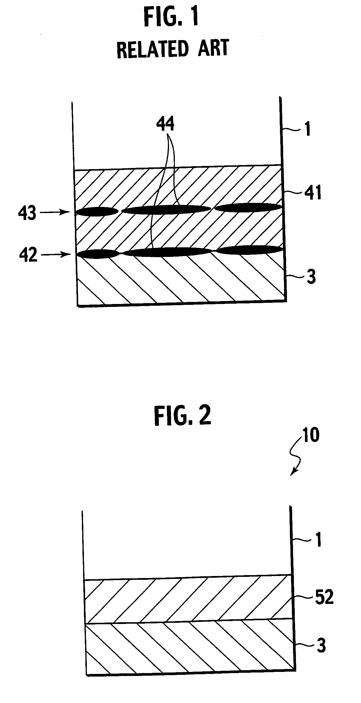
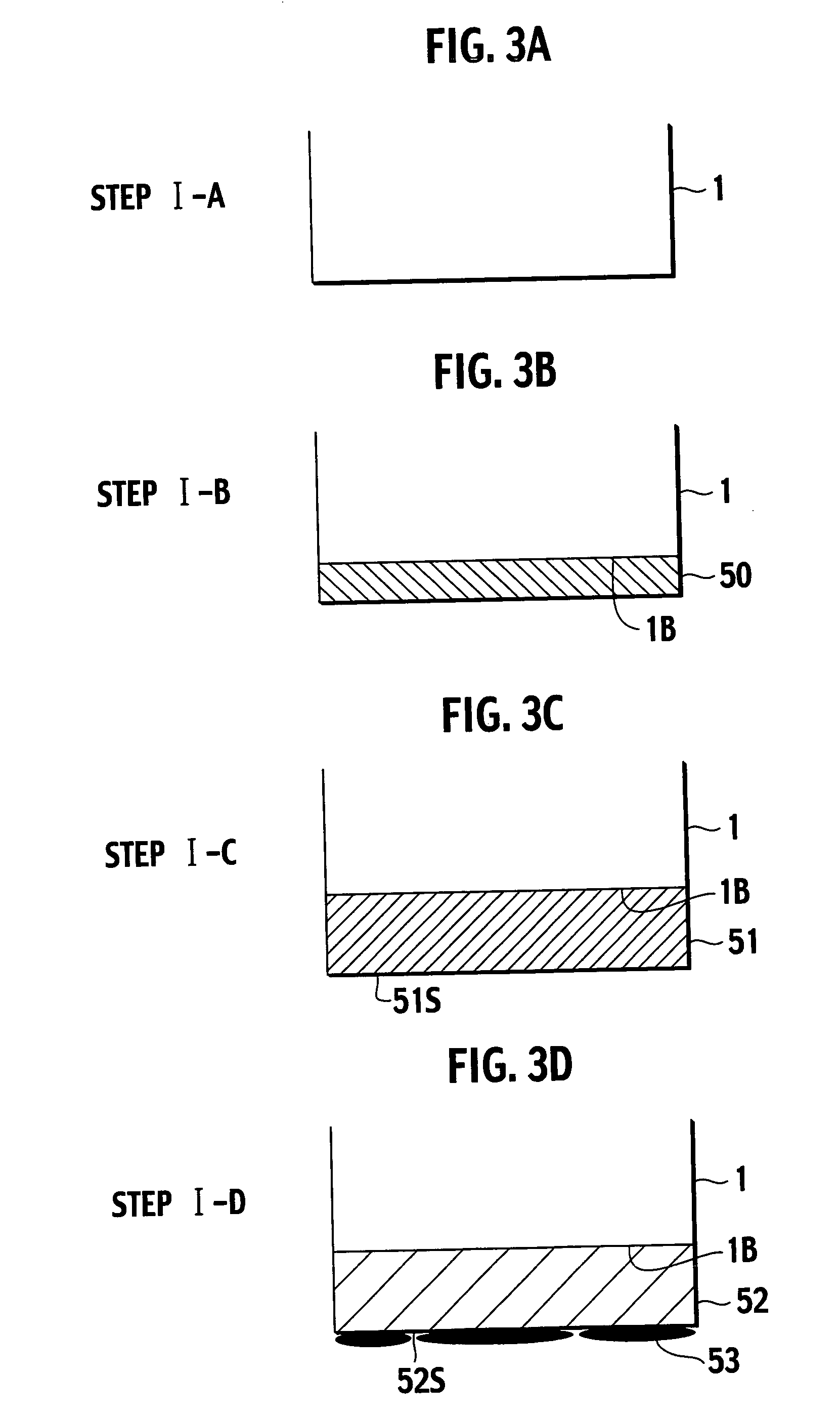
[0034]FIG. 2 shows a cross sectional view of an essential part of the silicon carbide semiconductor device 10, according to the first embodiment of the present invention. In FIG. 2, there is provided an n type 4H-SiC substrate 1 which is a silicon carbide substrate. At least a surface layer of a contact face of the n type 4H-SiC substrate 1 is doped with a high-concentration n type impurity. The substrate 1 has the contact face formed with a lower carbon content silicide electrode 52 (for example, NiSi2) which is formed by a contact annealing (solid phase reaction) and has a carbon content smaller than silicon content in mol number. The carbon content in mol number is ⅕ or less the silicon content, or preferably 1 / 10 or less the silicon content. ...

second embodiment

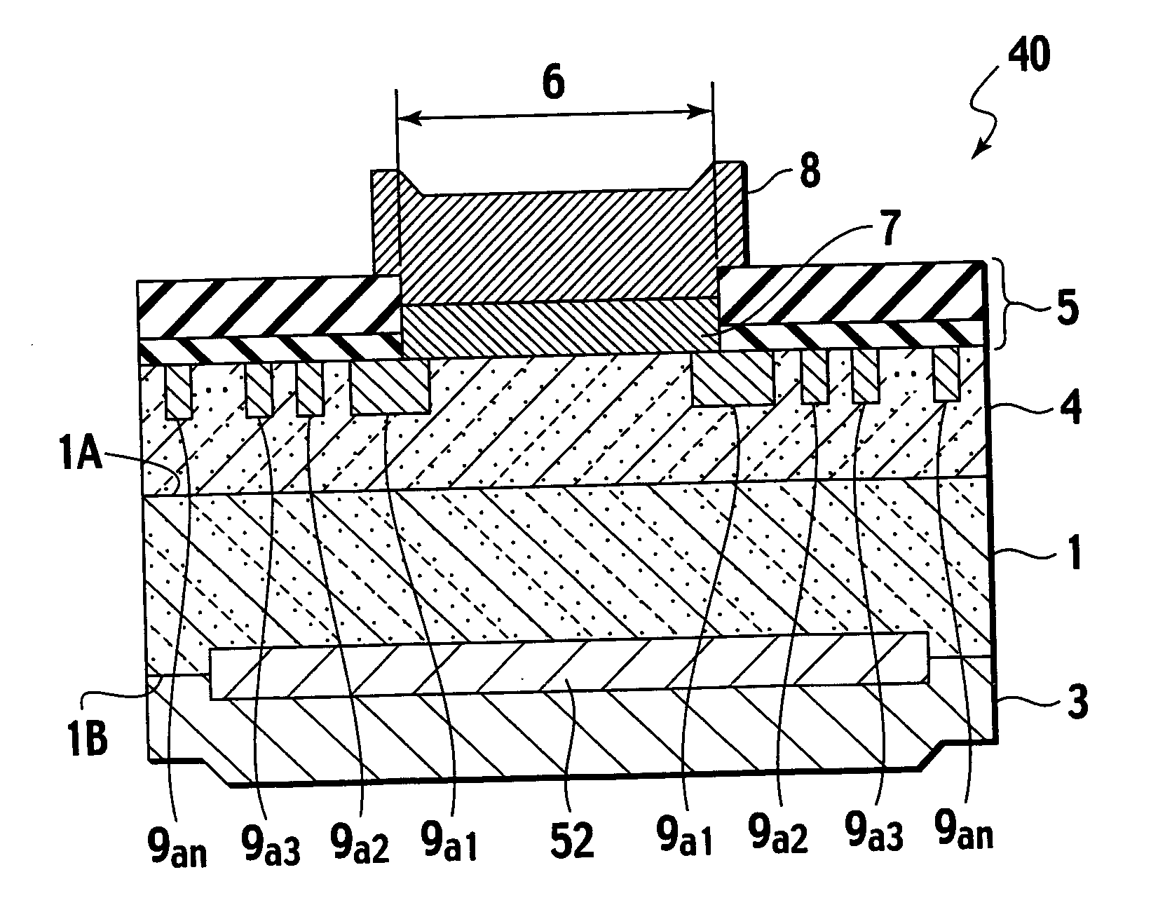
[0062] According to a second embodiment, the present invention is applied to a vertical Schottky diode which is a 2-terminal type device.

[0063]FIG. 4 shows a cross sectional view of an essential part of the vertical Schottky diode which is the silicon carbide semiconductor device 40, according to the second embodiment of the present invention. There is provided an n+ type single crystal 4H-SiC substrate 1 which is a silicon carbide substrate having impurity concentration of 1×10¹⁹ / cm3 or more. The n+ type single crystal 4H-SiC substrate 1 has the main surface 1A (upper in FIG. 4), that is, (0001) Si face where a first n− type epitaxial layer 4 having a thickness about 10 μm and added by nitrogen 5×10¹⁵ / cm3 is homo-epitaxially grown.

[0064] In a certain region of a surface layer of the n− type epitaxial layer 4, annular p type electric field relieving regions 9a1, 9a2, 9a3 to 9an each having a width of 2 μm are formed at a distance of 2 μm through an ion implantation and activation ...

third embodiment

[0090] According to a third embodiment of the present invention, there is provided a vertical MOSFET (Metal-Oxide-Semiconductor Field Effect Transistor) which is a type of 3-terminal switching device. Moreover, the 3-terminal switching device has a silicide electrode type ohmic contact on both of a main surface 71A and a main backface 71B of an SiC substrate 71, according to the third embodiment of the present invention.

[0091]FIG. 6 shows a cross sectional view of an essential part of a unit cell 70 of an SiC semiconductor MOSFET which is a silicon carbide semiconductor device 200, according to the third embodiment of the present invention. The unit cell 70 is a minimum unit of an active region. In a power element, many of the unit cells 70 are laterally arranged for greater current. Hereinafter, the reference numeral 70 is used for denoting both of the active region and the unit cell.

[0092] There is provided an n+ type single crystal 4H-SiC substrate 71 which is a silicon carbide...


PUM


Abstract

A silicon carbide semiconductor device, includes: 1) a silicon carbide substrate; 2) a silicide electrode configured to be formed by depositing a contact parent material on the silicon carbide substrate in such a manner as to cause a solid phase reaction, the silicide electrode being a lower carbon content silicide electrode including: i) silicon, and ii) carbon smaller than the silicon in mol number; and 3) an upper conductor film deposited to the silicide electrode.

Description

BACKGROUND OF THE INVENTION [0001] 1. Field of the Invention [0002] The present invention relates to a silicon carbide semiconductor device and a method for producing the same. 2. Description of the Related Art [0003] Semiconductor silicon carbide (SiC) has excellent features such as high electric breakdown field, high saturation electron velocity, high thermal conductivity, high heat resistance, high chemical stability, tough mechanical strength and the like. In addition, the semiconductor silicon carbide can form a pn junction and grow a thermally oxidized silicon film. Therefore, the semiconductor silicon carbide is the semiconductor material that realizes a ultra-low loss power device, a high frequency power amplifying device, a high temperature operation switching device and the like which cannot be achieved by Si. The semiconductor silicon carbide having the above features has been expected from the past and a basic research thereof has been done continuously. Recently, with c...

Claims


Application Information

Patent Timeline
IPC IPC(8): H01L31/0312
CPCH01L21/0465H01L21/0495H01L29/1608H01L29/6606H01L29/66068H01L21/0485H01L29/45
Inventor TANIMOTO, SATOSHI
Owner NISSAN MOTOR CO LTD
Why Eureka
Try Eureka