[0014] The following detailed description and the accompanying drawings provide a better understanding of the nature and advantages of the present invention.
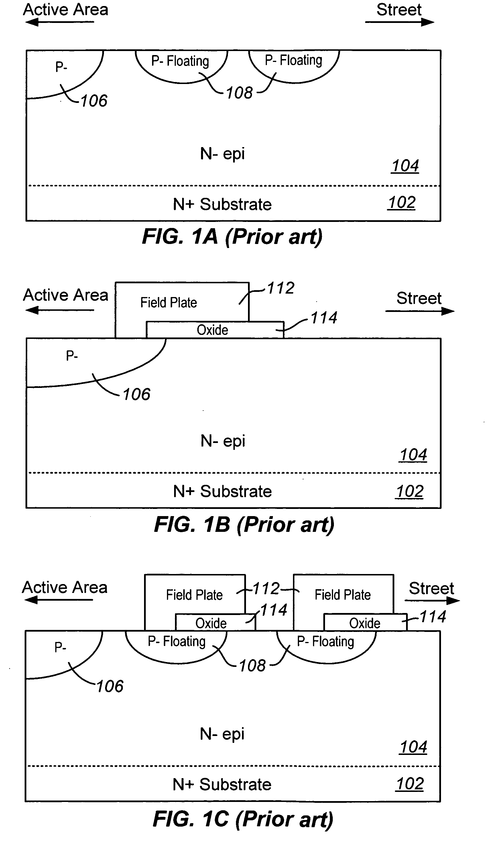
[0015]FIGS. 1A-1C show simplified cross-section views of three conventional termination structures;
[0016]FIGS. 2-9 show simplified cross-section views of various trench field plate termination structures in accordance with embodiments of the invention; and
[0017]FIGS. 10 and 11 show
simulation results for two different trench filed plate termination structures.
[0018] In accordance with the invention, various cost-effective termination techniques disclosed herein can be incorporated in various types of power devices, and which integrate particularly well with
trench gate FET technology.
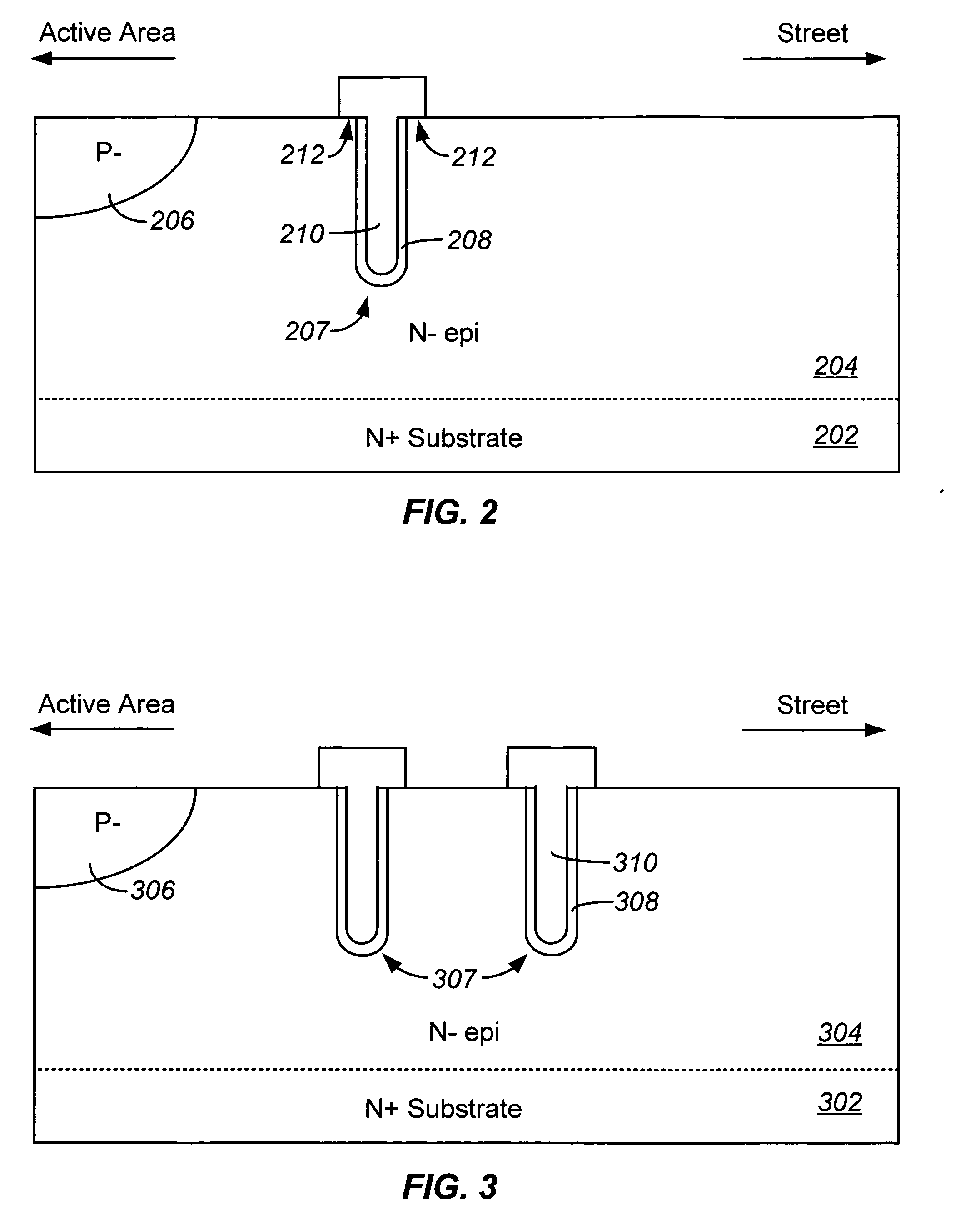
[0019]FIG. 2 is a simplified cross section view illustrating a termination technique in accordance with an embodiment of the invention. An N-type epitaxial layer 204 extends over an N-type substrate 202. A trench field plate structure 207 extends into epitaxial layer 204 and surrounds the active area of the die. P-type
diffusion region 206 represents the last blocking
diffusion of the active region of the die. Trench field plate 207 includes an insulating layer 208 (e.g., comprising
oxide) lining the trench sidewalls and bottom. Field plate 207 further includes P-type
electrode 210 (e.g., comprising polysilicon or epitaxially grown silicon) filling the trench and extending out of the trench to electrically contact epitaxial layer 204 surface regions 212 adjacent the trench. In general,
electrode 210 needs to be of a
conductivity type opposite that of the silicon region it contacts so that electrode 210 can bias itself. In this manner, trench field plate 207 more effectively spreads the electric fields during device operation, thus achieving a high
breakdown voltage.
[0020] In one embodiment, highly doped N-type regions flank each side of trench filed plate 207 in order to provide a better contact between electrode 210 and N-type epitaxial layer 204. While FIG. 2 shows trench field plate 207 extending deeper than P-type junctions 206, the invention is not limited as such. Factors determining the optimum depth of trench field plate 207 include the thickness of
dielectric layer 208 and the spacing between trench 207 and P-type region 206.
[0021] In one embodiment trench field plate 207 is formed as follows. A termination trench surrounding an active region of a power device is formed in epitaxial layer 204 using conventional silicon etch techniques. The trench is lined with an insulating layer 208 along its sidewalls and bottom using known techniques. An electrode 210 of opposite conductivity type to the epitaxial layer is formed using conventional
photolithography and
processing steps such that electrode 210 fills the trench and extends out to electrically contact adjacent surface regions of the epitaxial layer. In one embodiment, electrode 210 comprises P-type polysilicon formed using conventional poly deposition techniques. In another embodiment, electrode 210 is formed using conventional selective epitaxial growth (SEG) techniques.
[0022] As can be seen, trench field plate 207 is simple to form and consumes far less silicon area than the conventional floating rings and planar filed plate shown in FIGS. 1A-1C. In one embodiment, the termination technique in FIG. 2 is incorporated in a conventional
trench gate MOSFET. In this embodiment, many of the same
photolithography and
processing steps for forming the
trench gate structures in the active region are used to form trench field plate 207. Thus, a highly effective termination structure which consumes minimal silicon area and has minimal
impact on the manufacturing process is formed.
[0023]FIG. 3 illustrates a variation of the FIG. 2 embodiment wherein multiple trench field plates 307 are used to extend the
depletion region further away from the
transistor surface. An even higher breakdown
voltage is thus obtained. While only two trench field plates are shown, more trench field plate terminations can be used.
[0024]FIG. 4 shows a simplified cross-section view of another trench field plate termination structure 409 wherein a portion of epitaxial layer 406 is removed so that P-type region 406 terminates at a substantially vertically extending wall. The curvature of the P-type region as in, for example, P-type diffusion 306 in FIG. 3, is advantageously eliminated. As shown, the trench formed as a result of the silicon etch extends into the street (regions separating adjacent dice on a
wafer), though it may also be formed so as to terminate before reaching the street. A trench field
plate electrode 410 partially extends over and electrically contacts P-type region 406. Field
plate electrode 410 further extends vertically along the sidewall of floating region 406 and horizontally over the recessed surface of epitaxial layer 404. A
dielectric layer 408 (e.g., comprising
oxide) insulates filed
plate electrode 410 from epitaxial layer 404.
[0025] In one embodiment, the trench field plate structure 409 in FIG. 4 is formed as follows. After forming P-type region 406 in epitaxial layer 404 using conventional
implant / drive in techniques, an outer portion of epitaxial layer 404 surrounding the active region is recessed to below the depth of P-type region 406 using conventional
photolithography and silicon etch techniques. Insulating layer 408 is then formed using known techniques.
Electrode 410 is then formed using conventional photolithography and processing steps such that electrode 410 partially extends over and electrically contacts P-type regions 406, steps down along the sidewall of P-type region 406, and extends over the recessed surface of epitaxial layer 404.
[0026] In one embodiment, electrode 410 comprises a heavily doped polysilicon or epitaxially grown silicon. In another embodiment, prior to forming electrode 410, a heavily doped P-type diffusion region is formed in P-type region 406 at the interface between P-type region 406 and field plate electrode 410 so as to lower the
contact resistance between P-type region 406 and electrode 410. In another embodiment, P-type region 406 may be a floating region thereby enabling electrode 410 to bias itself. In this embodiment, electrode 410 and region 406 need to be of opposite conductivity type. In yet another embodiment, because the curvature of P-type diffusion region 406 is eliminated, diffusion region 406 need not be floating and may instead be an extended portion of the outer P-type well region of the active area.

