Time-of-light flight type distance sensor

a technology of time-of-light flight and distance sensor, which is applied in the direction of distance measurement, radiation controlled devices, instruments, etc., can solve the problems of (1) not working well, increased cost of ccd-cmos manufacturing procedure, limited application fields of (1) methods, etc., and achieves high performance range-finding, low cost, and maximum performance

Inactive Publication Date: 2007-07-12
NAT UNIV CORP SHIZUOKA UNIV
View PDF5 Cites 135 Cited by
  • Summary
  • Abstract
  • Description
  • Claims
  • Application Information

AI Technical Summary

Benefits of technology

[0012] It is preferable to manufacture a range-finding sensor with a maximum performance at low cost, by adding the least possible number of fabrication processes to a standard CMOS manufacturing procedure.
[0013] An object of

Problems solved by technology

Since the method of (1) cannot work well without a sufficient light intensity that facilitates generation of a pulse signal from the received signal, application fields of method of (1) are limited.
Such integrated CCD-CMOS manufacturing procedure increases cost.
Furthermore, while only a one-dimensional sensor (i.e., line sensor) is disclosed, implementation of a two-dimensional sensor (area sensor) established only with CCDs may be difficult, considering that all of the pixels should be simultaneously driven at a hig

Method used


Image

  • Time-of-light flight type distance sensor
  • Time-of-light flight type distance sensor
  • Time-of-light flight type distance sensor

Examples


first embodiment

[0028] Complete transfer of charges is required to provide a time-of-flight (hereafter, called ‘TOF’) sensor. However, it has been considered impossible to achieve such complete transfer using a standard CMOS architecture. Accordingly, some fabrication processes have been added to the standard CMOS manufacturing procedure. The present invention is to overcome such a problem by using a micro-fabrication technology and a special structure that can be fabricated using standard CMOS manufacturing procedure.

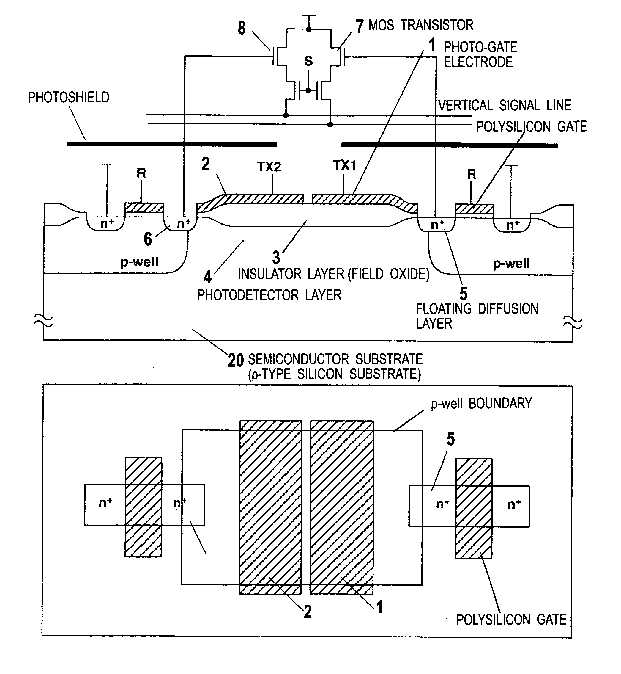
[0029]FIG. 1 shows a structure of a pixel of a range-finding sensor according to the present invention. While a single pixel may be used by itself for a certain application field, arranging a plurality of pixels one-dimensionally or two-dimensionally implements a range-finding sensor. FIG. 1(a) shows a cross-sectional view of the pixel of the range-finding sensor while FIG. 1(b) shows a plan view observed from above a surface of a semiconductor substrate—observed from a location in t...

second embodiment

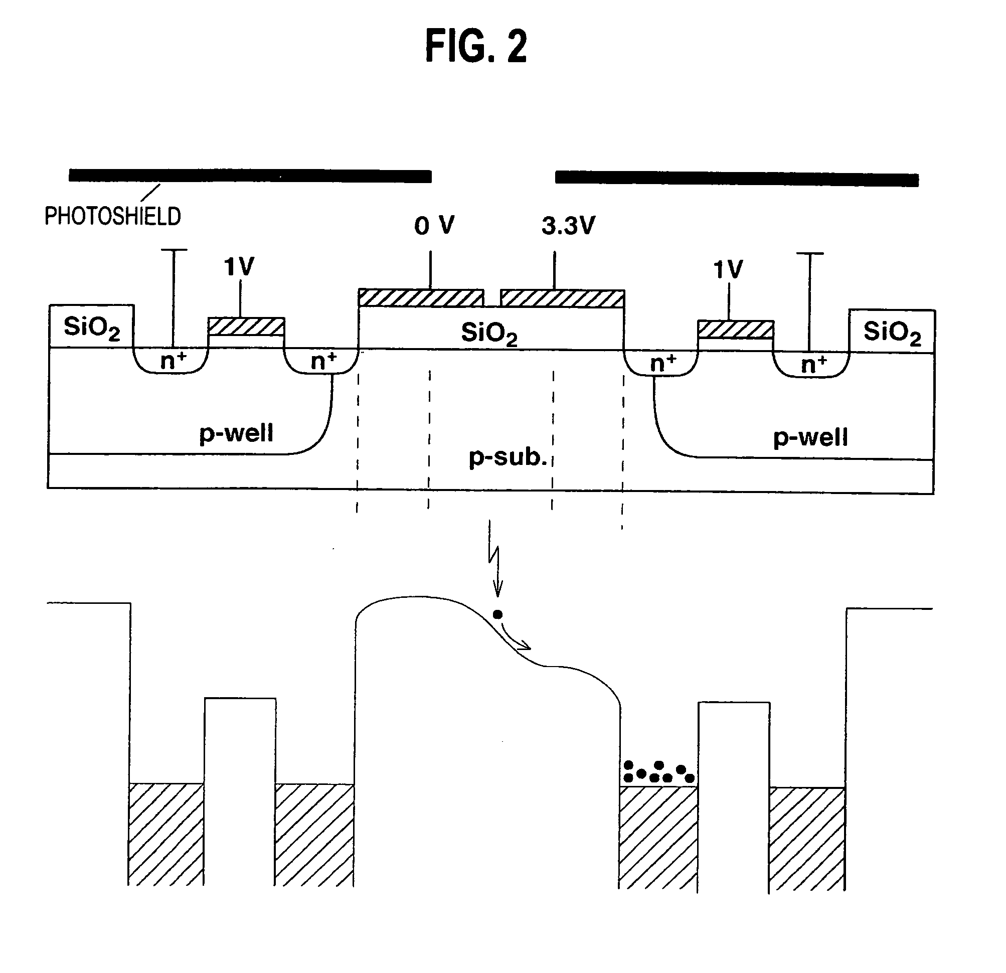
[0044] The structure of FIG. 2 is easily influenced by a background light (if it exists). That is, according to FIG. 2, even when reading out a signal, charges due to the background light are included in the signal, and furthermore, the times required for reading out the charges due to the background light differ in respective horizontal lines. This makes it difficult to perform background light removal processing. To avoid the difficulty in the background light removal processing, the read-out period needs to be sufficiently short relative to the TOF operating time, and thus high-speed read-out is required.

[0045]FIG. 5 shows a structure of a pixel circuit that is not influenced by the background light when reading out a signal. FIG. 6 is a timing chart for canceling the influence of the background light by reading out only signals due to the background light.

[0046] MOS transistors (9 and 10) are prepared on the right and the left side, respectively, so as to separate two floating...

third embodiment

[0052] In a structure shown in FIG. 1, if a fabrication process of forming another n-type diffusion layers under the field oxide is available, a structure of connecting the photodetector layer to the floating diffusion layers, which serve as the sources (or drains) of the MOS transistors via the n-type diffusion layers is possible, as shown in FIG. 7. When a wide (along the depth direction to the plane of the paper) gate width of a photodetector layer is designed so as to ensure a sufficiently large optical detection area, the greater the area of the high-concentration source or drain region of the MOS transistor, the more the dark current increases and the more the capacitance also increases, decreasing the voltage sensitivity. Therefore, as shown in FIG. 7, the n-type diffusion layers are provided so that the n-type diffusion layers can capture electrons generated in the photodetector layer.

[0053] Note that an n-type well layer may be used as the n-type diffusion layer being form...


PUM


Abstract

A lower cost range-finding image sensor based upon measurement of reflection time of light with reduced fabrication processes compared to standard CMOS manufacturing procedures. An oxide film is formed on a silicon substrate, and two photo-gate electrodes for charge-transfer are provided on the oxide film. Floating diffusion layers for taking charges out from a photodetector layer are provided at the ends of the oxide film, and on the outside thereof are provided a gate electrode for resetting and a diffusion layer for providing a reset voltage.

Description

FIELD OF THE INVENTION [0001] The present invention relates to a range-finding sensor, which measures a delay time of a light pulse transmitted from a light source and then reflected by a target object to be measured. BACKGROUND-ART [0002] The following references show related arts: [0003] (1) Inventor: Cyrus Bamji, Assignee: Canesta Inc., “CMOS-Compatible Three-dimensional image sensor”, U.S. Pat. No. US6323942 B1, Nov. 27, 2001; [0004] (2) R. Lange, P. Seitz, A. Biber, and S. Lauxtermann, “Demodulation pixels in CCD and CMOS technologies for time-of-flight ranging”, Proceedings of SPIE, Vol. 3965, pp. 177-188, 2000; [0005] (3) Ryohei Miyagawa, Takeo Kanade, “CCD-based range-finding sensor”, IEEE Trans. Electron Devices, vol. 44, No. 10, pp. 1648-1652 (1997); [0006] (4) Range Imaging Device, Japanese Patent Application Laid-open No. 2001-281336; and [0007] (5) Charge Coupled Device, Japanese Patent Application Laid-open No. 2003-51988. [0008] According to the method of (1), light p...

Claims


Application Information

Patent Timeline
IPC IPC(8): H01L27/14G01C3/06G01S7/481G01S7/4863G01S17/10G01S17/894H01L27/144H01L27/146H01L31/02H04N13/00
CPCG01S7/4816G01S17/10H01L27/14603H01L27/14609H01L27/14643G01S7/4863H04N5/335H04N13/0207H04N13/0253G01S17/89H04N3/155H04N13/254H04N13/207G01S17/894G01C3/06G01S17/00H01L27/14
Inventor KAWAHITO, SHOJI
Owner NAT UNIV CORP SHIZUOKA UNIV
Why Eureka
Try Eureka