Liquid Crystal Display Device

Active Publication Date: 2007-07-12
PANASONIC LIQUID CRYSTAL DISPLAY CO LTD +1
View PDF21 Cites 31 Cited by
  • Summary
  • Abstract
  • Description
  • Claims
  • Application Information

AI Technical Summary

Benefits of technology

[0049] By thus introducing a layer(s) having anisotropic absorption into a liquid crystal display device, it is possible to achieve the improvement of the degree of polarization by assistance to the degree of polarization of polarizing plates, compensation for the nonuniformity of the degree of polarization, and the reduction of the luminance and bluishness of a black display by the absorption of leaked light.
[0050] In the present invention, when a dichromatic compound is added to a color filter layer to impart dichroism, it is more effective to make the transmission wavelength region of the color filter layer substantially the same as the absorption wavelength region of the dichromatic compound. When such an anisotropic absorption is present on a substrate on the observer side, the change of tones at the time of black display can be compensated for without a marked change of tones at the time of white display by making the axis of absorption of the anisotropic absorption substantially parallel to the axis of absorption of a polarizing plate located on the observer side. Thus, the invention is effective. When the aforesaid anisotropic absorption is present on a substrate on the light source side, the long-term stability of orientation-regulating force can be attained by making the axis of absorption of the anisotropic absorption substantially parallel to the axis of absorption of a polarizing plate located on the light source side. Thus, the present invention is effective.
[0051] In the present invention, as a light source, there may be used light-emitting units such as

Problems solved by technology

The reason is considered as follows: it is difficult to control the order parameters of the resin and iodine completely.
This intensification is disadvantageous in the liquid crystal televisions in which the presentation of a black color is considered important.
In the liquid crystal display devices adopting this TN method, the narrow angle of field of view is considered the greatest problem.
Particularly in IPS-TFT-LCD having many level difference structures on the surfaces facing the liquid crystal layer, it is difficult to subject the alignment films to uniform alignment treatment all over a large screen.
As the fibers, there are very fine fibers of several microns, but cloth made of such very fine fibers has not been put to practical use because the cloth for rubbing is required to have stiffness for applying a certain degree of frictional force.
Therefore, rubbing near the level difference is insufficient, so that the orientation tends to be disturbed.
This disturbance of the orientation causes a rise of the black level and a lowering of the image quality (e.g. a decrease in contrast ratio and the nonuniformity of luminance) due to the rise.
However, owing to the level difference between wirings extending in definite directions (e.g. the signal wiring electrodes, common electrodes in a pixel and pixel electrodes) and their ends, the fibers are drawn in the direction of the level difference from a preset angle, so that the orientation is disturbed, resulting in a lowering of the image quality, such as a rise of the black level.
Therefore, the disturbance of orientation tends to be conspicuous as compared with other methods.
On the other hand, the IPS method is sensitive to the disturbance of an initial orientation state because in this method, dark level display is carried out at low or zero voltage.
Therefore, such a method becomes sensitive to the disturbance of the direction of initial orientation.
Thus, in the IPS method, the uniformity of orientation is a very important factor and problems in the rubbing method adopted at present are becoming clear.
In general, rubbing alignment treatment involves many problems concerning a rubbing treatment method, such as TFT damage caused by static electricity generated by friction, unsatisfactory display due to the disturbance of orientatio

Method used


Image

  • Liquid Crystal Display Device
  • Liquid Crystal Display Device
  • Liquid Crystal Display Device

Examples


first embodiment

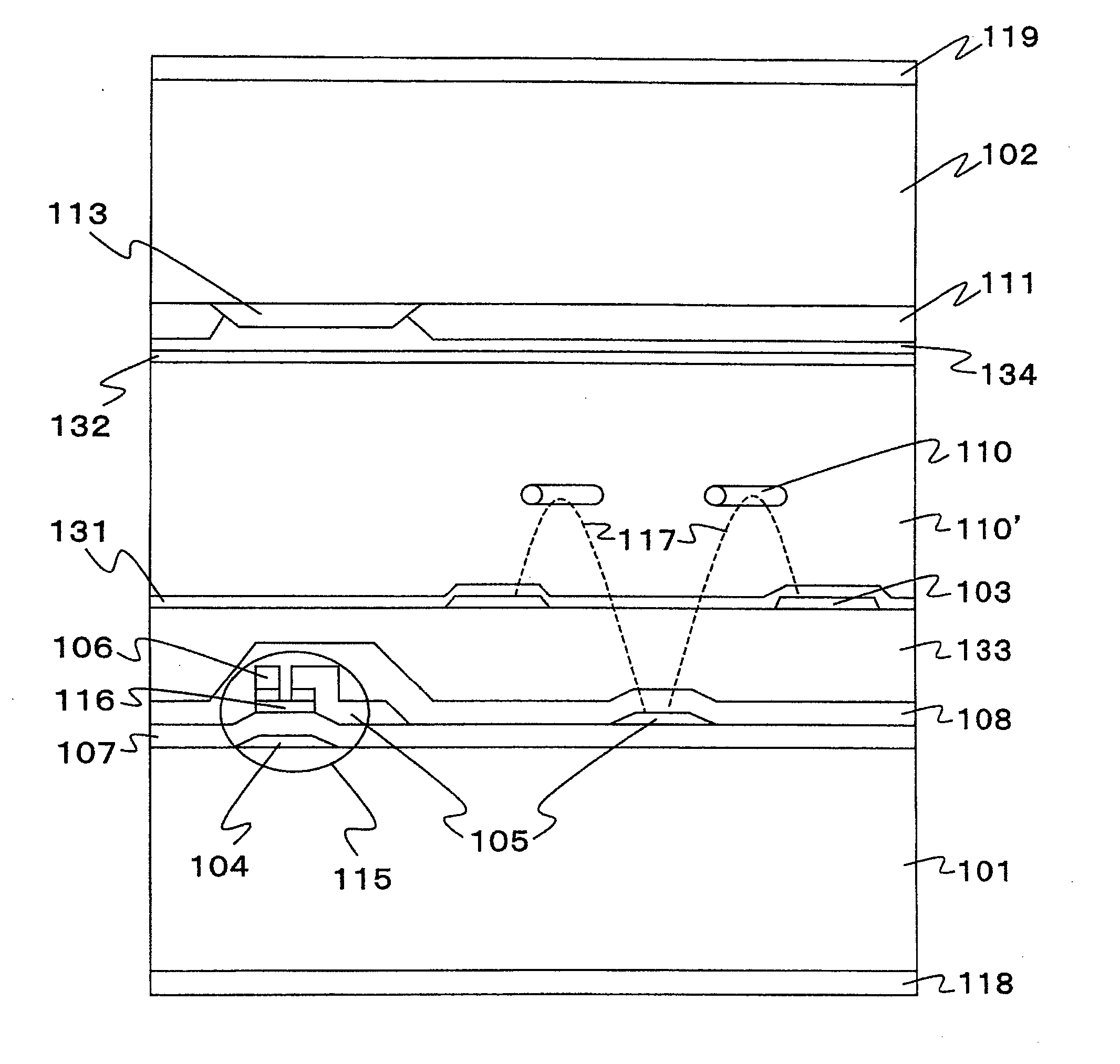
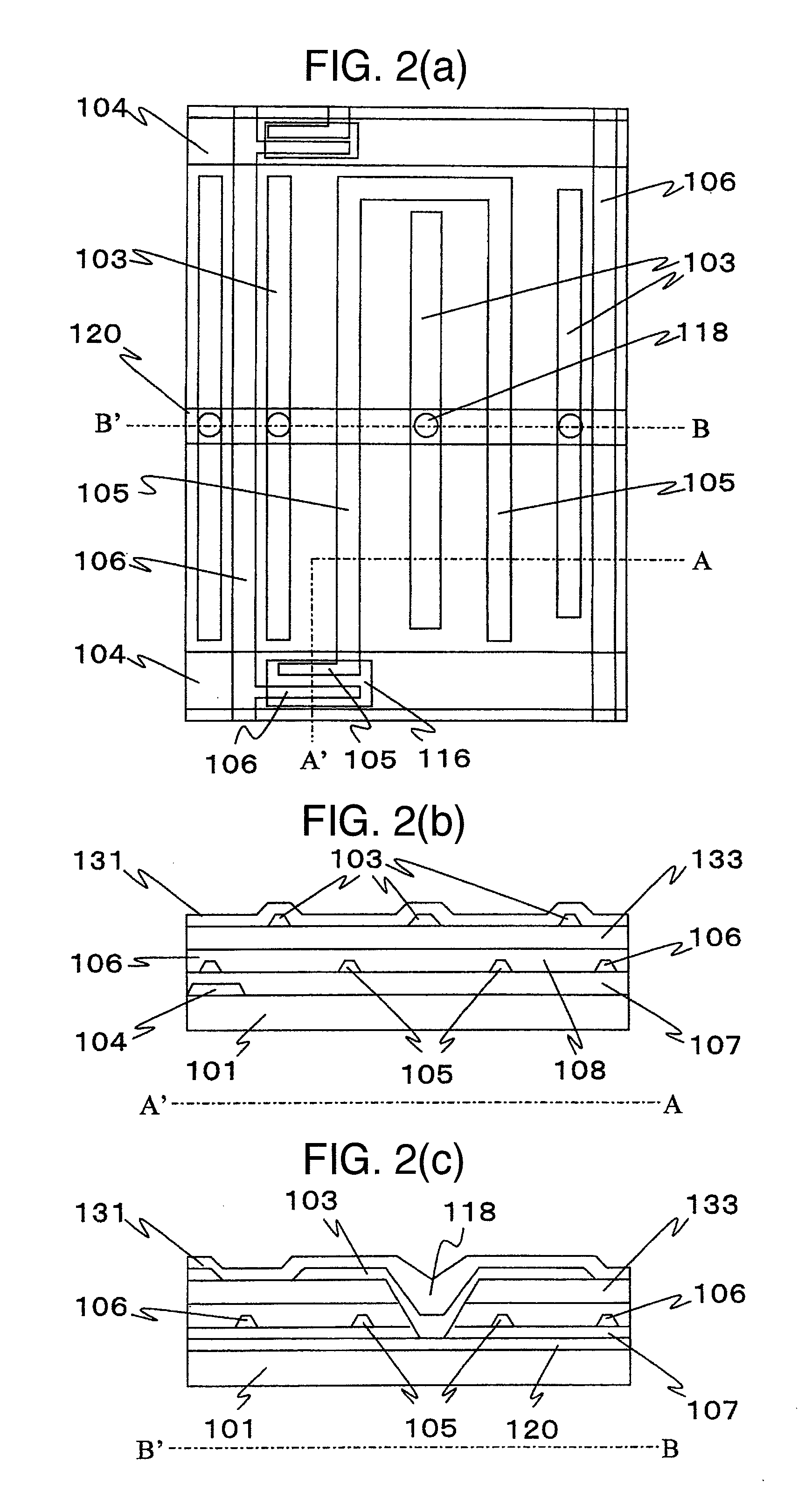
[0066]FIG. 1 is a schematic cross-sectional view of the vicinity of a pixel which illustrates a first embodiment of the liquid crystal display device of the present invention. FIG. 2 is schematic views of an active-matrix substrate for explanation of the structure of the vicinity of a pixel which illustrate the first embodiment of the liquid crystal display device of the present invention. FIG. 2(a) is a plan view, FIG. 2(b) is a sectional view taken along the line A-A′ in FIG. 2(a), and FIG. 2(c) is a sectional view taken along the line B-B′ in FIG. 2(a). FIG. 1 corresponds to a part of a section along the line A-A′ in FIG. 2(a). The sectional views as FIG. 2(b) and FIG. 2(c) are schematic views in which the structure of the main portion is emphasized, and they do not correspond to the sections along the line A-A′ and the line B-B′, respectively, in FIG. 2(a) in an one-by-one manner. For example, in FIG. 2(b), a thin-film transistor 115 is not shown, and in FIG. 2(c), only a portio...

second embodiment

[0079] A second embodiment of the liquid crystal display device of the present invention is explained below. FIG. 3 is a schematic cross-sectional view of the vicinity of a pixel which illustrates the second embodiment of the liquid crystal display device of the present invention. FIG. 4 is schematic views of an active-matrix substrate for explanation of the structure of the vicinity of a pixel which illustrates the second embodiment of the liquid crystal display device of the present invention. FIG. 4(a) is a plan view, FIG. 4(b) is a sectional view taken along the line A-A′ in FIG. 4(a), and FIG. 4(c) is a sectional view taken along the line B-B′ in FIG. 4(a). FIG. 3 shows a part of a section along the line A-A′ in FIG. 4(a). The sectional views as FIG. 4(b) and FIG. 4(c) are schematic views in which the structure of the main portion is emphasized, and they do not correspond to the sections along the line A-A′ and the line B-B′, respectively, in FIG. 4(a) in an one-by-one manner. ...

third embodiment

[0089]FIG. 5 is a schematic cross-sectional view of the vicinity of a pixel which illustrates a third embodiment of the liquid crystal display device of the present invention. In FIG. 5, the same symbols as in the drawings in the embodiments described above correspond to the same functional portions as in these embodiments. As shown in FIG. 5, in the present embodiment, a pixel electrode 105 located under a protective film 108 is drawn up to the surface of an organic insulating film 133 through a through-hole 118 to be located at the same level as that of common electrodes 103. When this structure is used, a voltage for driving liquid crystals can be further reduced.


PUM

PropertyMeasurementUnit
Nanoscale particle sizeaaaaaaaaaa
Wavelengthaaaaaaaaaa

Abstract

An object of the present invention is to provide a liquid crystal display device that has an excellent mass-productivity and gives an image improved by the reduction of the chromaticity difference between white display and black display, the reduction of coloring and luminance in black display, and the improvement of the contrast ratio. In the present invention, of a pair of alignment films 131 and 132 formed on a pair of substrates 101 and 102, respectively, the alignment film 132 formed on the glass substrate 102 on the observer side is made of a material obtained by adding a photoisomerized compound to a photosensitive polymer and has anisotropic absorption all over the visible light wavelength region (approximately 400 nm to 750 nm).

Description

BACKGROUND OF THE INVENTION [0001] The present invention relates to liquid crystal display panel substrates having a member having anisotropic absorption, and liquid crystal display devices such as liquid crystal display panels using the substrates. [0002] The range of use of liquid crystal displays is increasing because they are characterized, for example, in that they have a high display quality, are thin and consume only low electric power. In recent years, there is a growing demand for a good color reproducibility and a high contrast ratio with an increase of the range of use of the liquid crystal displays as mobile monitors (e.g. monitors for mobile phone and monitors for digital still camera), monitors for desktop personal computers, monitors for printing and design, medical monitors and liquid crystal televisions. Particularly in the case of the liquid crystal televisions, the presentation of a black color is considered very important and a high luminance is urgently required...

Claims


Application Information

Patent Timeline
IPC IPC(8): C09K19/00
CPCC08G73/10C09K19/02C09K2323/02C09K2323/031G02F1/133723G02F1/133788G02F1/134363G02F1/133738
Inventor MATSUMORI, MASAKITAMIOKA, YASUSHIKUNIMATSU, NOBORU
Owner PANASONIC LIQUID CRYSTAL DISPLAY CO LTD
Why Eureka
Try Eureka