Group-iii nitride semiconductor laser device, and method for fabricating group-iii nitride semiconductor laser device
Inactive Publication Date: 2011-06-02
SUMITOMO ELECTRIC IND LTD
View PDF6 Cites 19 Cited by
Summary
Abstract
Description
Claims
Application Information
AI Technical Summary
This helps you quickly interpret patents by identifying the three key elements:
Problems solved by technology
Method used
Benefits of technology
Benefits of technology
[0011]In this group-III nitride semiconductor laser device, a thickness of the support base is in a range of not less than 50 μm and not more than 100 μm. When the thickness is not less than 50 μm, handling becomes easier, and production yield becomes higher. When the thickness is not more than 100 μm, it is more preferred for obtaining good-quality fractured faces for a laser cavity.
[0023]In this method, the semipolar principal surface is any one of {20-21} plane, {10-11} plane, {20-2-1} plane, and {10-1-1} plane. With these semipolar surfaces, it is also feasible to provide the first and second end faces with flatness and perpendicularity enough to construct the laser cavity of the group-III nitride semiconductor laser device, or without ion damage.
Problems solved by technology
However, when the laser waveguide extends in this orientation, there are no appropriate crystal facets suitable for the laser cavity mirrors, and it is thus difficult to form good laser cavity mirrors by the conventional technology making use of cleavage.
When the angle is in a range of more than 80° and less than 100°, it might result in failing to achieve desired flatness and perpendicularity.
Method used
Image
Click on the blue label to locate the original text in one second.
Reading with bidirectional positioning of images and text.
Examples
example 1
[0094]A GaN substrate with a semipolar surface is prepared, and perpendicularity of a fractured facet is observed as described below. The above substrate used has a {20-21}-plane GaN substrate formed by cutting a (0001) GaN ingot, thickly grown by HYPE, at the angle of 75° to the m-axis. The principal surface of the GaN substrate is mirror-finished, and the back surface has pear-skin which is finished by grinding. The thickness of the substrate is 370 μm.
[0095]On the back side in the pear-skin state, a scribed groove is formed perpendicularly to the projected direction of the c-axis on the principal surface of the substrate, with a diamond pen, and thereafter the substrate is fractured by press. For observing the perpendicularity of the resultant fractured face, the substrate is observed from the a-plane direction with a scanning electron microscope.
[0096]Part (a) of FIG. 7 shows a scanning electron microscope image of the fractured face observed from the a-plane direction, and the ...
example 2
[0097]It is found in Example 1 that in the GaN substrate having the semipolar {20-21} plane, the fractured face obtained by forming the scribed groove perpendicular to the projected direction of the c-axis on the principal surface of the substrate and by pressing the substrate, has the flatness and perpendicularity in the principal surface of the substrate. For estimating applicability of this fractured face to the laser cavity, a laser diode shown in FIG. 8 is grown by organometallic vapor phaseepitaxy as described below. The raw materials used are as follows: trimethyl gallium (TMGa); trimethyl aluminum (TMAl); trimethyl indium (TMIn); ammonia (NH3); and silane (SiH4). A substrate 71 is prepared. A GaN substrate is prepared as the substrate 71, and the GaN substrate is cut with a waferslicing apparatus at an angle in a range of 0° to 90° to the m-axis from a (0001) GaN ingot thickly grown by HVPE, in such a manner that the angle ALPHA of the c-axis tilted toward the m-axis has a...
example 3
[0112]In Example 2, the plurality of epitaxial films for the semiconductor laser are grown on the GaN substrate having the {20-21} surface. As described above, the end faces for the optical cavity are formed through the formation of scribed grooves and by press. In order to find candidates for these end faces, plane orientations different from the a-plane and making an angle near 90° with respect to the (20-21) plane are obtained by calculation. With reference to FIG. 13, the following angles and plane orientations have angles near 90° with respect to the (20-21) plane.
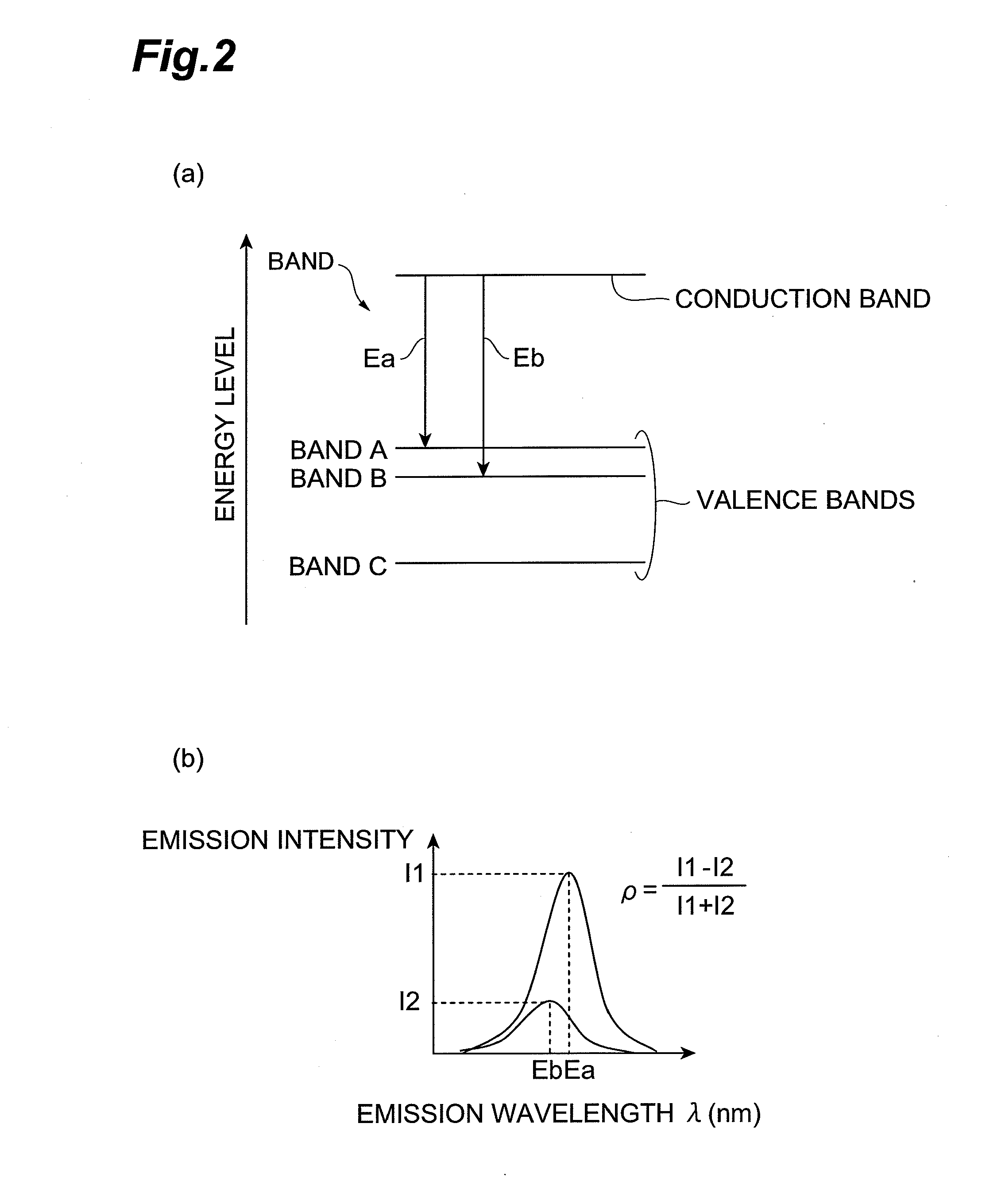
Specific plane index,Angle to {20-21} plane;(-1016),92.46°;(-1017),90.10°;(-1018),88.29°
[0113]FIG. 14 is a drawing showing atomic arrangements in the (20-21) plane, (−101-6) plane, and (−1016) plane. FIG. 15 is a drawing showing atomic arrangements in the (20-21) plane, (−101-7) plane, and (−1017) plane. FIG. 16 is a drawing showing atomic arrangements in the (20-21) plane, (−101-8) plane, and (−1018) plane. As shown...
PUM
Abstract
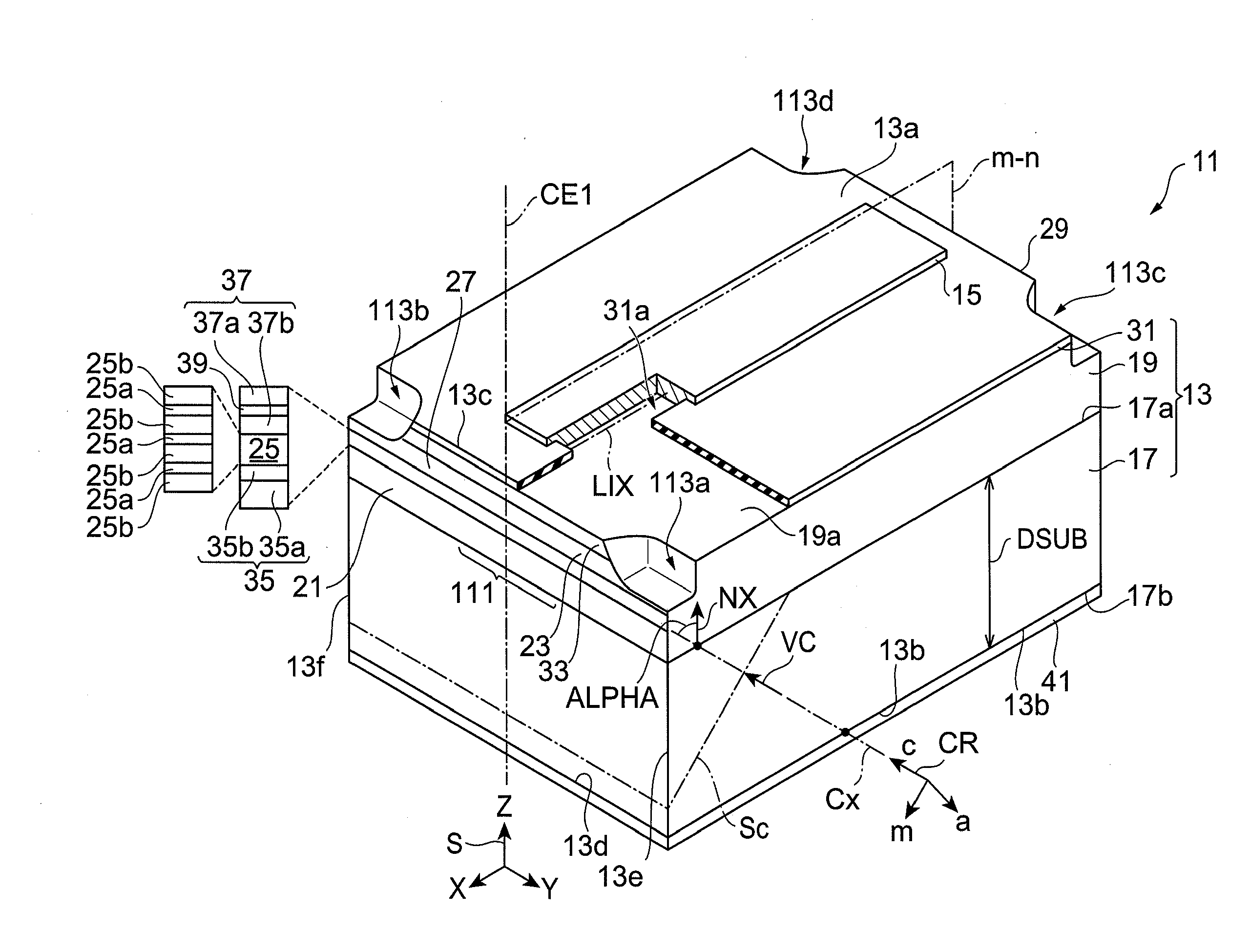
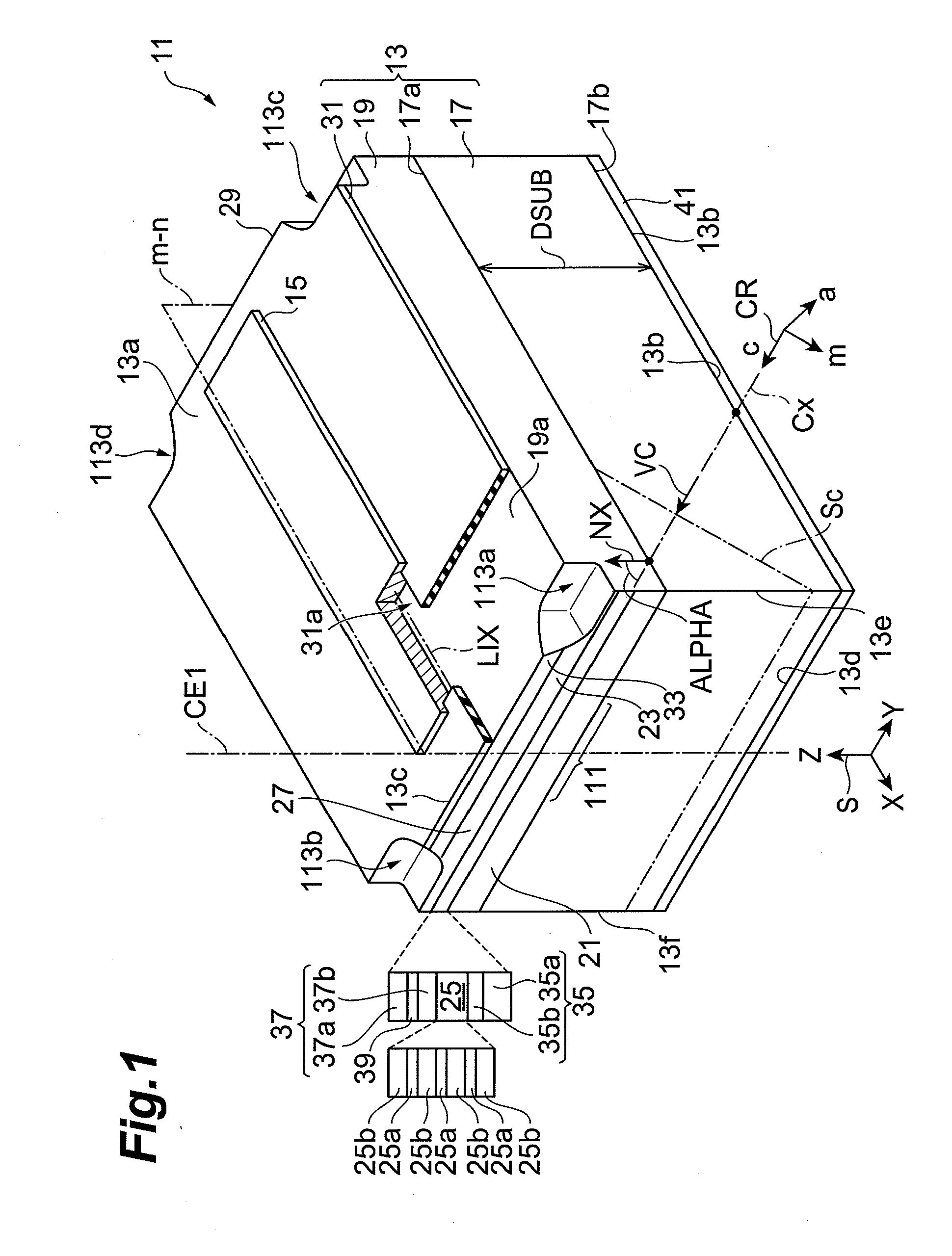
Provided are a group-III nitridesemiconductorlaser device with a laser cavity to enable a low threshold current on a semipolar surface of a hexagonal group-III nitride, and a method for fabricating the group-III nitridesemiconductorlaser device on a stable basis. Notches, e.g., notch 113a and others, are formed at four respective corners of a first surface 13a located on the anode side of a group-III nitride semiconductor laser device 11. The notch 113a or the like is a part of a scribed groove provided for separation of the device 11. The scribed grooves are formed with a laser scriber and the shape of the scribed grooves is adjusted by controlling the laser scriber. For example, a ratio of the depth of the notch 113a or the like to the thickness of the group-III nitride semiconductor laser device 11 is not less than 0.05 and not more than 0.4, a tilt of a side wall surface at an end of the notch 113a is not less than 45° and not more than 85°, and a tilt of a side wall surface at an end of the notch 113b is not less than 10° and not more than 30°.
Description
BACKGROUND OF THE INVENTION[0001]1. Field of the Invention[0002]The present invention relates to a group-III nitride semiconductor laser device, and a method for fabricating the group-III nitride semiconductor laser device.[0003]2. Related Background Art[0004]Patent Literature 1 (Japanese Patent Application Laid-open No. 2009-117494) discloses a method for fabricating a semiconductor device, comprising a step of forming first auxiliary grooves in a semiconductor device structure provided on a semiconductor substrate; a step of forming second auxiliary grooves in the semiconductor device structure; and a step of dividing the semiconductor substrate and the semiconductor device structure in division directions along the first auxiliary grooves and the second auxiliary grooves. In this fabrication method, a plurality of second auxiliary grooves are separately provided in the division directions, and at least two first auxiliary grooves are provided separately from each other between at...
Claims
Application Information
Patent Timeline
Application Date:The date an application was filed.
Publication Date:The date a patent or application was officially published.
First Publication Date:The earliest publication date of a patent with the same application number.
Issue Date:Publication date of the patent grant document.
PCT Entry Date:The Entry date of PCT National Phase.
Estimated Expiry Date:The statutory expiry date of a patent right according to the Patent Law, and it is the longest term of protection that the patent right can achieve without the termination of the patent right due to other reasons(Term extension factor has been taken into account ).
Invalid Date:Actual expiry date is based on effective date or publication date of legal transaction data of invalid patent.

