Structure matter of thin-film particles having carbon skeleton, processes for the production of the structure matter and the thin-film particles and uses thereof

a technology of structure matter and thin-film particles, which is applied in the direction of water-setting substance layered product, chemistry apparatus and processes, transportation and packaging, etc., can solve the problems of poor position selectivity, inability to propose concrete methods, and degradation of semiconductor parts, etc., and achieves simple and clean methods, high electric conductivity, and easy utilization of electronic nature or stability

Inactive Publication Date: 2007-07-12
HIRATA MASUKAZU +2
View PDF10 Cites 21 Cited by
  • Summary
  • Abstract
  • Description
  • Claims
  • Application Information

AI Technical Summary

Benefits of technology

[0145] The structure matter composed of the thin film particles having a carbon skeleton (carbon nanofilms in oxidized form and in reduced form) and the substrate on which the thin film particles are mounted, provided by the present invention, is a novel system that can easily utilize the electronic nature or stability peculiar to a carbon material having a periodic structure. It can be applied to fine circuits (device or wiring), circuits for high temperatures (device or wiring), opto-electric conversion devices (solar cell, light-emitting device, etc.), exothermic matters, optical devices, stable recording materials and the like.
[0146] According to the present invention, the thin film particles obtained by oxidizing graphite can be reduced by a simple and clean method. The reduction gives thin film particles having high electric conductivity and the thin film particles are remarkably useful as a conductor or a semiconductor in various uses.
[0147] Further, the thin film particles having a carbon skeleton, provided by the present invention, have high mobility and function as an ambipolar. Further, an economical technique such as spincoating, screen printing or inkjet printing can be used for the formation of a film. The obtained film is almost free from the occurrence of pinholes and structurally stable and has high heat resistance. From these characteristics, various high functional semiconductor devices can be actualized.
[0148] The present invention will be explained more in detail with reference to Examples hereinafter, while the present invention shall not be limited to these Examples.

Problems solved by technology

However, these methods have problems such as poor position selectivity, degradation of a semiconductor part due to a need of heating at a high temperature for a long period of time, and the like.
However, concrete methods therefor have not been proposed.
However, when the reduction is carried out by heating, the whole of the thin film layer is heated so that it is difficult to selectively reduce only the specific part.
However, when the above thin film particles are taken out from the dispersion and then reduced by heating, the particles adhere to each other to undergo aggregation so that the previous dispersed state can not be held.
However, steps of removal of the reducing agent used and purification are complicate so that the above method is not preferable.
However, the mobility of the organic semiconductive material is low at the present stage, which prevents it from going in to actual use.
However, it is difficult to form a film from a solution since they are not easily dissolved in an organic solvent.
Therefore, an expensive vapor-deposition apparatus is necessary so that it is disadvantageous in view of a cost.
Further, it is difficult to form a homogeneous film in a broad domain by vapor deposition.
The vapor deposition is not suitable for forming a large-area film.
However, the mobility is generally low.
However, most of these materials have a low glass transition temperature and are apt to undergo crystallization.
Therefore, it is difficult to obtain a stable device by using these compounds as an electron transport material.
Further, “New development of organic EL” at page 6 in the 2001 August issue of “Kinou Zairyo” published by CMC Publishing Co., Ltd., has a description indicating that hole transport materials and electron transport materials with high mobility are not present, which is a cause to use an ultrathin film difficult to form.
However, although various materials have been proposed as an organic semiconductor material, there has not been yet obtained an organic semiconductor material having sufficient properties.

Method used


Image

  • Structure matter of thin-film particles having carbon skeleton, processes for the production of the structure matter and the thin-film particles and uses thereof
  • Structure matter of thin-film particles having carbon skeleton, processes for the production of the structure matter and the thin-film particles and uses thereof
  • Structure matter of thin-film particles having carbon skeleton, processes for the production of the structure matter and the thin-film particles and uses thereof

Examples


example 1

[0149] (Production of Oxidized Form Thin Film Particles Having a Planar-Direction Size of about 20 μm)

[0150] 10 g of natural graphite (supplied by SEC Corporation, SNO-25, purity 99.97 wt % or more, a refined article from which impurities, etc., were removed by heating at 2,900° C., average particle diameter 24 μm, particle diameter 4.6 μm or less 5 wt % and particle diameter 61 μm or more 5 wt %) was added to a Mixed liquid containing 7.5 g of sodium nitrate (purity 99%), 621 g of sulfuric acid (purity 96%) and 45 g of potassium permanganate (purity 99%), and the mixture was allowed to stand at about 20° C. for 5 days with stirring mildly, to obtain a high viscosity liquid. The high viscosity liquid was added to 1,000 cm3 of 5 wt % sulfuric acid aqueous solution (water having conductivity of less than 0.1 μS / cm was used for dilution (the same hereinafter)) over about 1 hour with stirring, and the resultant mixture was further stirred for 2 hours, to obtain a liquid. 30 g of hydrog...

example 2

[0218] The aqueous dispersion, having a concentration of 0.45 wt %, of the oxidized form thin film particles, which had an oxygen content of about 42 wt % and a hydrogen content of about 2 wt % according to the elemental analysis results of the particles after vacuum-drying at 40° C. and had a planar-direction size of about 20 μm, obtained in Example 1, was used as a dispersion A. The following experiments were carried out using the dispersion A.

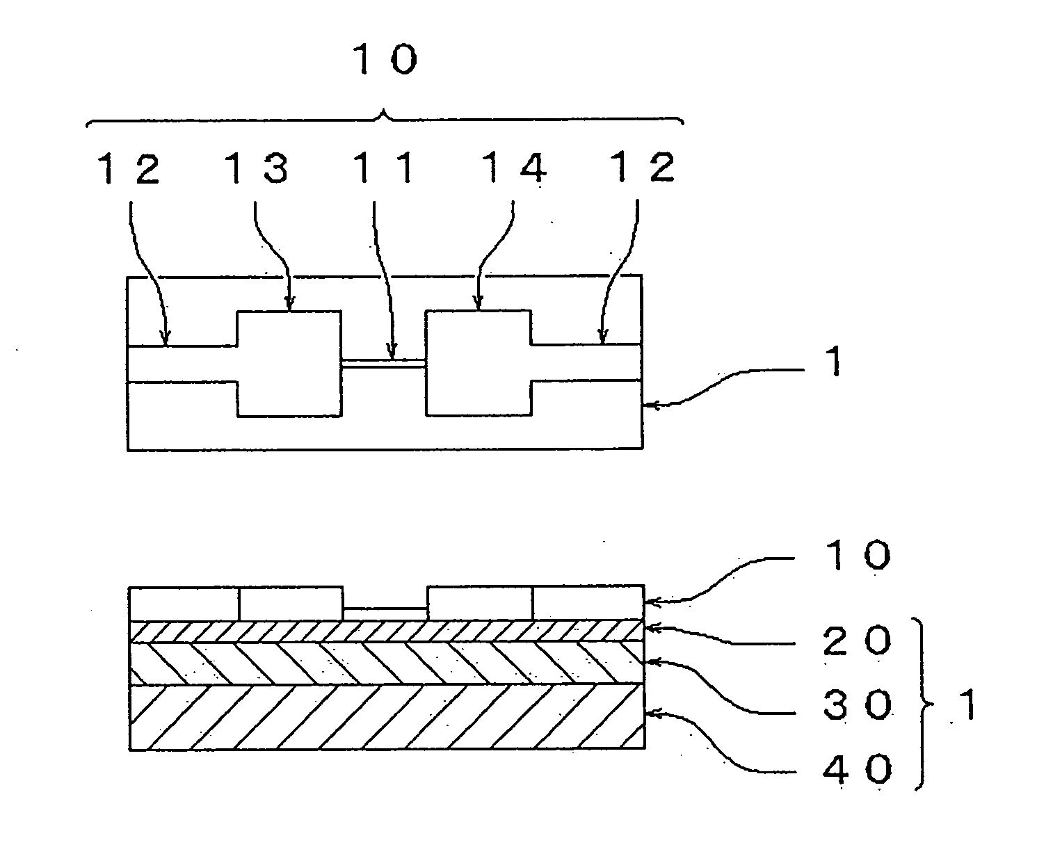
[0219] Two gold wiring lines were formed on a silica glass substrate at a space of 2 mm. A thin film layer formed of the thin film particles was formed such that the thin film layer straddled the two wiring lines. The film formation was carried out by dropping the dispersion A between the wiring lines with a pipet and drying the dispersion medium at 80° C. for 15 minutes. The thickness of the film after the drying was about 1 μm. The thus-obtained thin film layer was irradiated with light of an ultrahigh pressure mercury lamp (supplied by U...

example 3

[0221] Similarly to Example 2, the dispersion A was dropped between two gold wiring lines on a silica glass substrate, the dispersion was dried at 80° C. for 15 minutes to form an about 1 μm-thick thin film layer formed of the thin film particles. The thus-produced thin film layer was irradiated with light of a xenon lamp (300 W) from a distance of 15 cm. After irradiation for 40 minutes, the thin film layer was measured for resistance. The resistivity of the thin film particles was calculated from the measured resistance value, to find it was 1,500 Ω·cm. Further, the thin film layer was irradiated for 80 minutes and the resistivity became 50 Ω·cm.


PUM

PropertyMeasurementUnit
thicknessaaaaaaaaaa
relative dielectric constantaaaaaaaaaa
thicknessaaaaaaaaaa

Abstract

The present invention provides a structure matter composed of (a) oxidized form thin film particle(s) which are obtained by oxidizing graphite, have a thickness of 0.4 nm to 10 μm and a planar-direction size at least twice as large as the thickness, have lyophilic to a liquid having a relative dielectric constant of 15 or more and have a carbon skeleton or an oxidized form lamination layer aggregate in which the oxidized form thin film particles are combined with each other, or (b) reduced form thin film particle(s) or a reduced form lamination layer aggregate obtained by partially or completely reducing the above oxidized form thin film particle(s) or the above oxidized form lamination layer aggregate so as to have an oxygen content of 0 to 35 wt %, and (c) a substrate, the oxidized form thin film particle(s), the oxidized form lamination layer aggregate, the reduced form thin film particle(s) or the reduced form lamination layer aggregate being in contact with the substrate, its use and a method for reducing thin film particles having a carbon skeleton.

Description

FIELD OF THE INVENTION [0001] The present invention relates to a structure matter in which thin film particle(s) having a carbon skeleton are mounted on a substrate, processes for the production of the structure matter and the thin film particle(s), and uses of these. More specifically, it relates to a structure matter or thin film particles that can easily utilize the electronic nature or stability peculiar to a carbonaceous material having a periodic structure and production processes of these. The present invention can be applied to fine circuits (device or wiring), circuits for high temperatures (device or wiring), opto-electric conversion devices (solar cell, light-emitting device, etc.), semiconductor devices, exothermic matters, optical devices, stable recording materials and the like. PRIOR ARTS [0002] In recent years, searches for materials having high anisotropy of shape and applications thereof are proceeding rapidly. As an anisotropic shape material having carbon atoms a...

Claims


Application Information

Patent Timeline
Patent Type & Authority Applications(United States)
IPC IPC(8): B32B9/00B32B13/04H01L27/28H01L51/05H01L51/40
CPCH01L27/28Y10T428/30H01L51/0541H01L51/0021H10K19/00H10K71/60H10K10/464
Inventor HIRATA, MASUKAZUGOTOU, TAKUYAHORIUCHI, SHIGEO
Owner HIRATA MASUKAZU
Why Eureka
Try Eureka