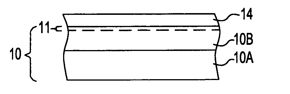
[0012] The present invention provides a method in which a high k dielectric material having a dielectric constant of greater than that of
silicon dioxide can be formed on a surface of a III-V compound semiconductor material with electrical properties sufficient for high-performance FET applications wherein the interface between the high k dielectric material and the III-V compound semiconductor material is of good quality, resulting in a low interface
state density (on the order of about 1012 cm−2 eV−1 or less); the unit for the interface state density can also be written as cm−2 / eV. That is, the present invention provides a method in which a high k dielectric material is formed on an unpinned, i.e. passivated, surface of a III-V compound semiconductor material. In accordance with the method of the present invention, the surface of the III-V compound semiconductor includes substantially no
oxide or other contaminants that would otherwise cause a large interface state density in the structure.
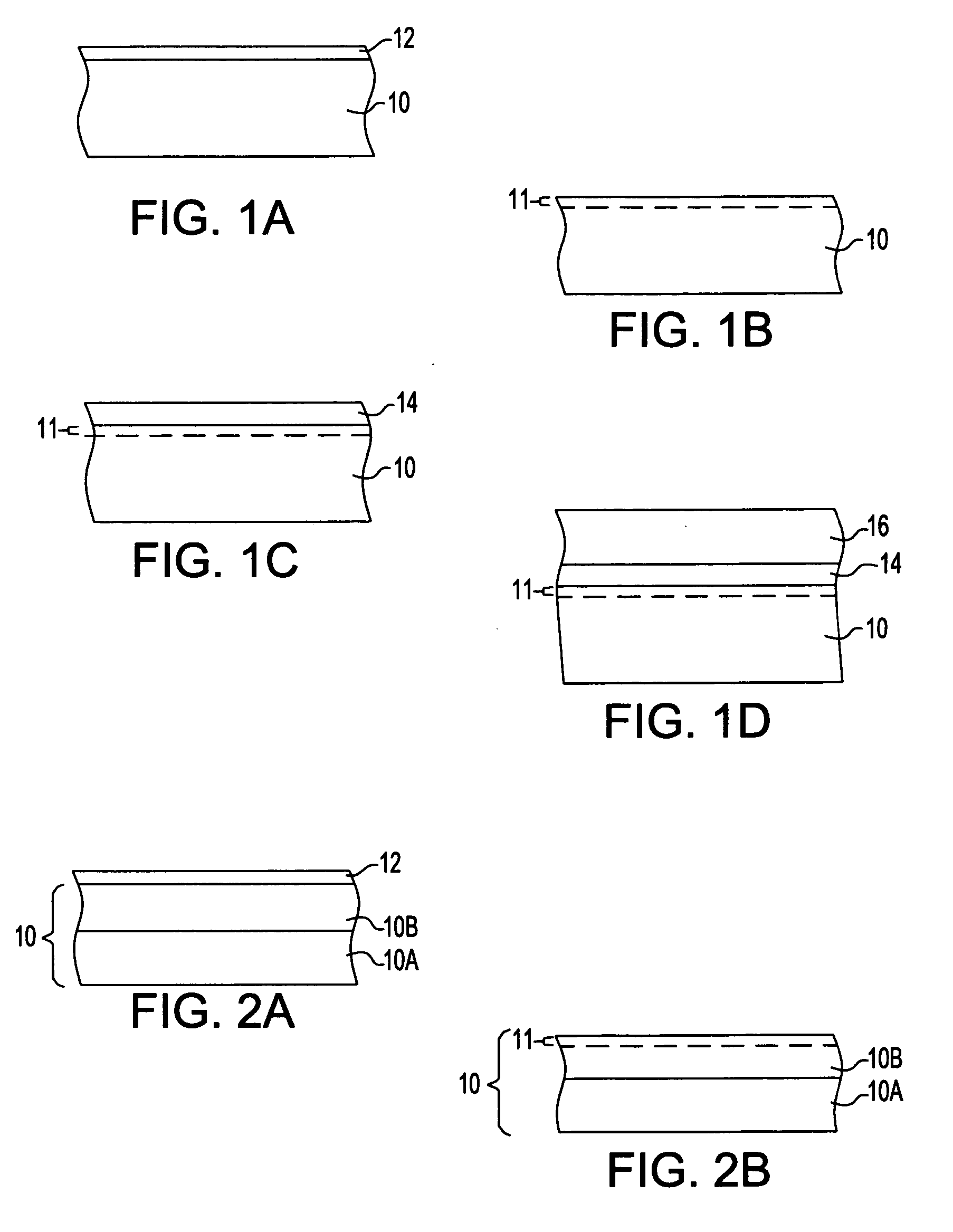
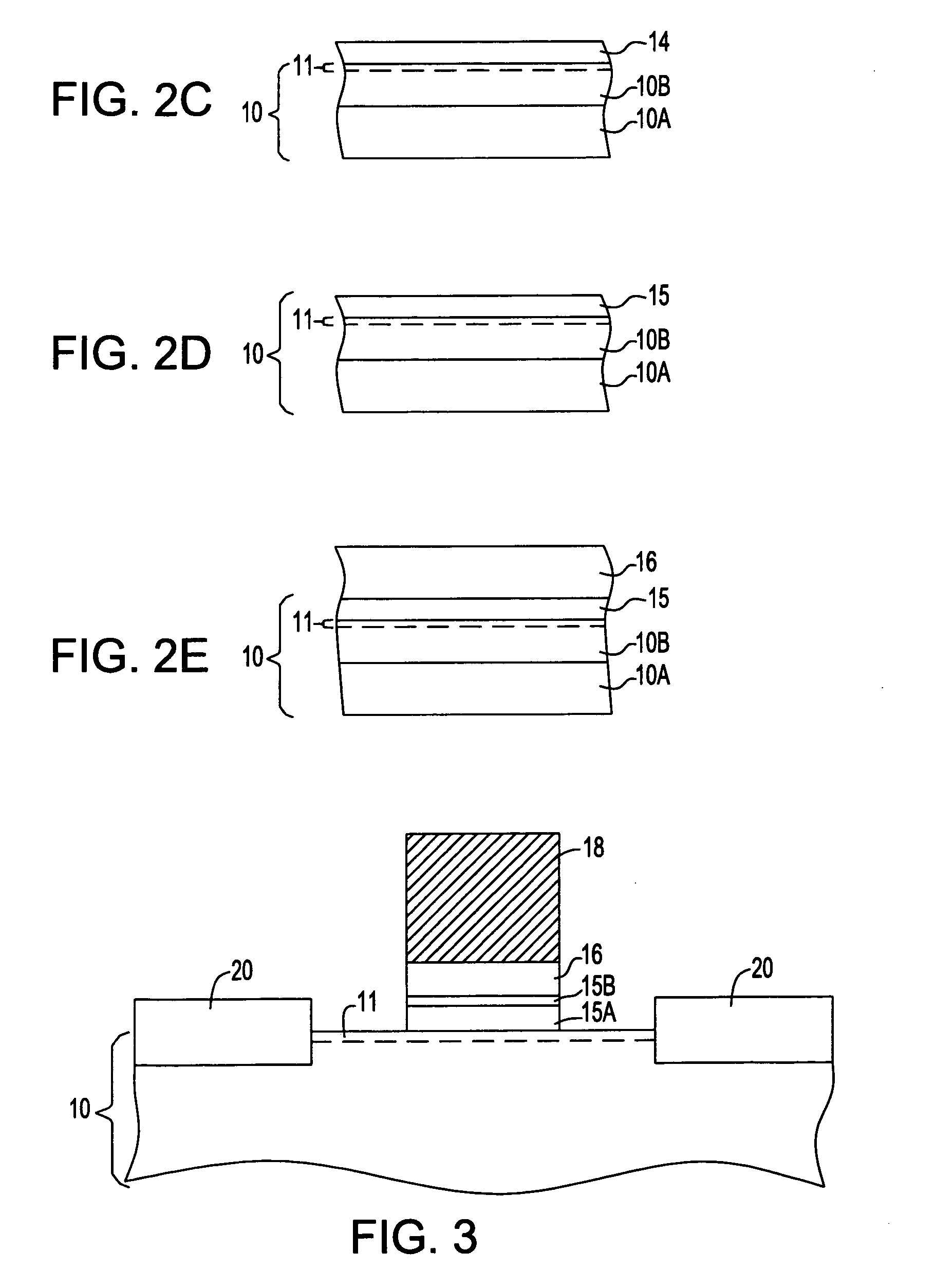
[0029] The methods of the present invention described above have has several advantages. First the semiconducting, e.g., Si, layer is excellent at passivating a surface of a III-V compound semiconductor material, particularly a GaAs surface. Secondly, by depositing the semiconducting layer using a high-quality technique such as MBE, the surface can be cleaned (either by desorbing the
oxygen at high temperatures, or using a H-
plasma preclean), to create a virtually
oxygen-
free interface. The semiconducting
layer thickness can be controlled to high precision as well, and thus be made very thin. If the semiconducting layer is nitridated, in situ, a
nitrogen plasma could be used to then convert the semiconducting layer to a semiconducting
nitride.
Nitride, instead of oxide, formation has the
advantage that over nitridation will not cause problems, as generally, nitridation of the GaAs surface does not degrade the electrical characteristics.
Over oxidation, on the other hand, can severely degrade the electrical characteristics. Once the
nitride is formed, the surface is stable against oxidation, and could be removed and exposed to air, for subsequent high k deposition. A semiconducting
nitride also has the
advantage of allowing the subsequent HfO2 that is deposited to nucleate amorphous as opposed to polycrystalline, which can improve the electrical properties. The HfO2 could be deposited in situ as well, which would have the
advantage that the entire
gate stack could be deposited in a single vacuum step. The inventive process has the additional advantage that it does not require a high-temperature step, as the H-preclean, semiconducting layer deposition, optional nitridation, oxidation or oxynitridation and high k deposition all could be performed at a temperature of less than 300° C., which would avoid any
contamination or surface degradation problems associated with sublimation of one of the elements of the III-V compound semiconductor material.

