Dual damascene process flow enabling minimal ULK film modification and enhanced stack integrity

a damascene and process flow technology, applied in the field of integrated circuits, to achieve the effect of facilitating the deposition of thin-polymer layers, sufficient selectivity, and increasing metal/ulk interconnect performan

Inactive Publication Date: 2007-07-12
GLOBALFOUNDRIES INC
View PDF18 Cites 27 Cited by
  • Summary
  • Abstract
  • Description
  • Claims
  • Application Information

AI Technical Summary

Benefits of technology

[0014] For single damascene such a permutation is straight-forward, however for dual damascene, this requires the diffusion barrier etching process to be specially tailored so as to achieve sufficient selectivity to the exposed trench ILD material (and potentially exposed hard mask films dependent on whether or not the via-fill organic material located in the field is completely consumed during the barrier / via-fill etch process) while etching the via-fill material and diffusion barrier. Such a process is potentially feasible for OSG materials comprising SiCOH-based low k materials (porous and / or nonporous) and for hard mask materials comprising typical inorganic films (oxide, TEOS, oxynitride, nitride). Since via-fill materials are typically organic and the diffusion barrier is of a SiC type (SiC, SiCH, SiCNH), etching chemistries comprising specifically tailored fluorine: oxygen gas ratios (<4:1) can be employed to produce desired dual damascene trench profiles; enabling the deposition of the sacrificial polymeric layer for wall protection through a permutation of the diffusion barrier open and ashing steps.
[0015] This permutation, for both single and dual damascene, facilitates the deposition of a thin-polymeric layer onto the sidewall of the trenches coating the OSG dielectric and, if present, the organic adhesion promoter with this thin layer. This thin layer of polymer achieves two key functional advantages, namely: (1) protects the exposed wall portions of the OSG dielectric from the subsequent plasma ashing chemistries and hence “damage” and (2) protects the organic adhesion promoter from consumption during ashing. In this manner, the degree of physical and chemical modification induced by the plasma ashing chemistry onto the OSG dielectric is reduced allowing increased metal / ULK interconnect performance and furthermore, the mechanical integrity of the stack is maintained since the organic adhesion promoter is relatively unscathed.
[0017] The present invention also provides an interconnect structure of improved RC electrical performance versus that of an interconnect structure built with conventional single or dual damascene processing. Also, the mechanical integrity of the OSG dielectric / diffusion barrier stack is improved.
[0020] The interconnect structure of the present invention further includes an optional hard mask located on a portion of an upper surface of the OSG dielectric and a diffusion barrier located on a portion of a lower surface of the OSG dielectric. In some embodiments of the present invention; an organic adhesion promoter is present between the OSG dielectric and the diffusion barrier. In accordance with the present invention, the underlying organic adhesion promoter is also not damaged and, as such, the integrity of the diffusion barrier and the OSG dielectric is maintained.

Problems solved by technology

Such an approach will lead to some (or all) of the issues highlighted above.

Method used


Image

  • Dual damascene process flow enabling minimal ULK film modification and enhanced stack integrity
  • Dual damascene process flow enabling minimal ULK film modification and enhanced stack integrity
  • Dual damascene process flow enabling minimal ULK film modification and enhanced stack integrity

Examples


Embodiment Construction

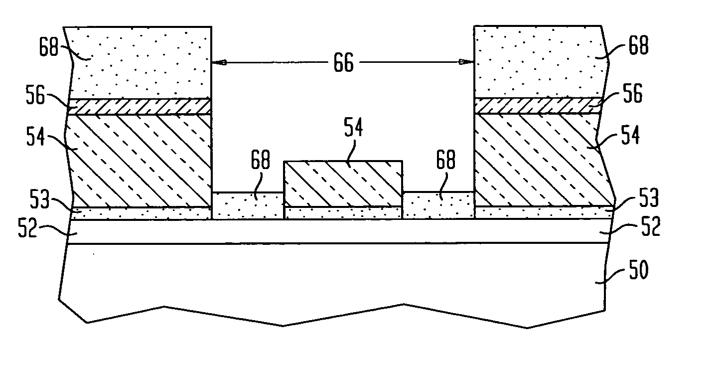
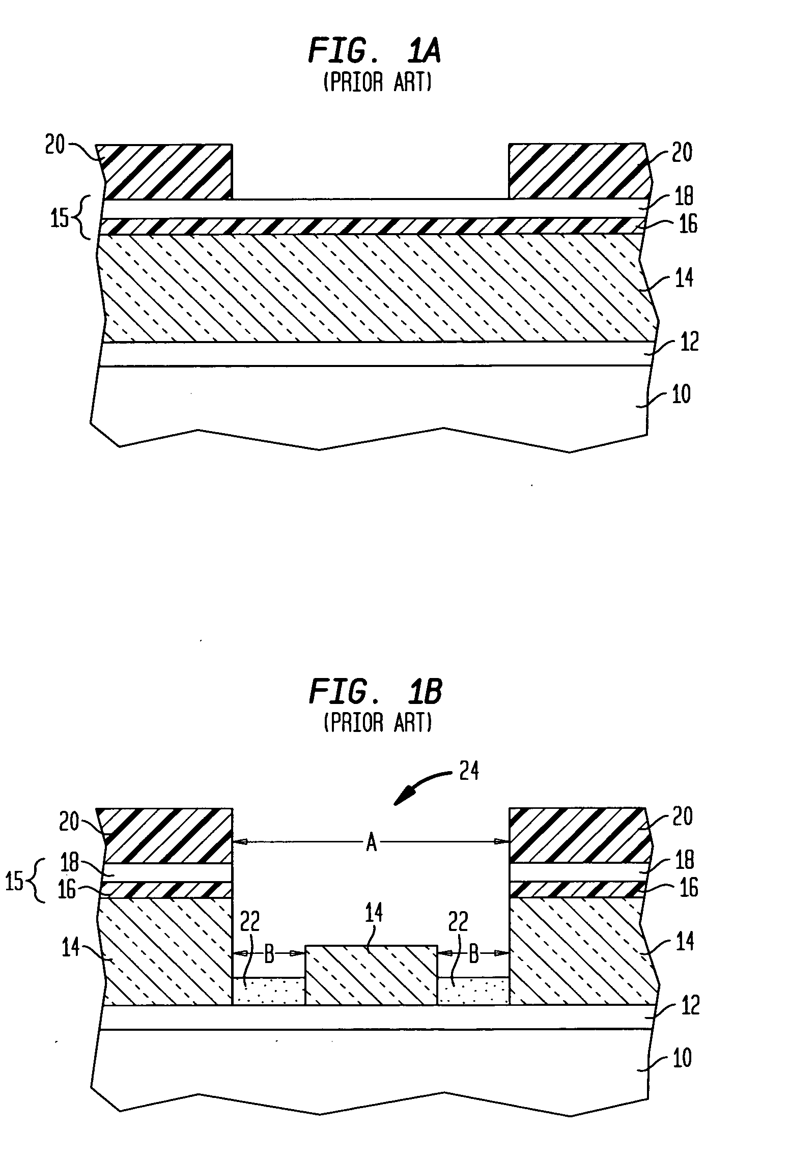
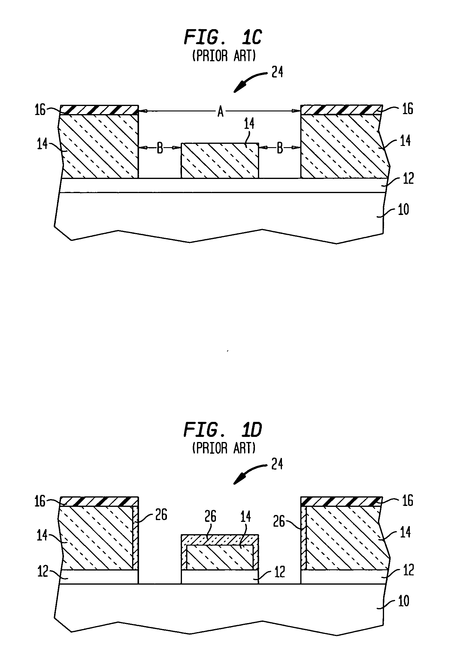
[0028] The present invention, which provides a dual damascene process enabling minimal OSG dielectric modification and enhanced stack integrity, will now be described in greater detail by referring to the following discussion and drawings that accompany the present application. It is noted that the drawings of the present application showing the processing flow of a conventional process and the inventive process are provided for illustrative purposes and, as such, they are not drawn to scale.

[0029] The present invention which is directed to an interconnect structure useful for forming a semiconductor device is built with an alternative single and dual damascene processing sequence in which the diffusion barrier open precedes the removal of the resist layer(s). Permuting the sequence of these two steps facilitates improved target metal / ULK interconnect electrical (RC) performance (reduced leakage) and mechanical integrity of the stack. Both of these are achieved as a sacrificial pol...


PUM

PropertyMeasurementUnit
dielectric constantaaaaaaaaaa
dielectric constantsaaaaaaaaaa

Abstract

Interconnect structures possessing an organosilicate glass interlayer dielectric material with minimal stoichiometeric modification and optionally an intact organic adhesion promoter for use in semiconductor devices are provided herein. The interconnect structure is capable of delivering improved device performance, functionality and reliability owing to the reduced effective dielectric constant of the stack compared with that of those conventionally employed because of the use of a sacrificial polymeric material deposited onto the dielectric and optional organic adhesion promoter during the barrier open step done prior to ashing the patterning material. This sacrificial film protects the dielectric and optional organic adhesion promoter from modification / consumption during the subsequent ashing step during which the polymeric film is removed.

Description

FIELD OF THE INVENTION [0001] The present invention generally relates to integrated circuits (ICs), and more particularly to interconnect structures, including multilevel interconnect structures, in which advanced dual damascene processing enables target ultra low k (ULK) interconnect performance and enhanced mechanical integrity (reliability). The terms “ultra low k” or “ULK” refer to an organosilicate glass having a dielectric constant of less than 3.0. The present invention also provides a method of fabricating an interconnect structure in which wall portions of the organosilicate glass (OSG) dielectric are not damaged during processing. BACKGROUND OF THE INVENTION [0002] Generally, semiconductor devices include a plurality of circuits that form an integrated circuit including chips (e.g., chip back end of line, or “BEOL”), thin film packages and printed circuit boards. Integrated circuits (ICs) can be useful for computers and electronic equipment and can contain millions of tran...

Claims


Application Information

Patent Timeline
Patent Type & Authority Applications(United States)
IPC IPC(8): H01L21/4763
CPCH01L21/76801H01L21/76829H01L21/76808
Inventor DALTON, TIMOTHY J.FULLER, NICHOLAS C.NITTA, SATYANARAYANA V.
Owner GLOBALFOUNDRIES INC
Why Eureka
Try Eureka