Forming integrated circuits using selective deposition of undoped silicon film seeded in chlorine and hydride gas

a technology of silicon film and selective deposition, applied in the field of selective deposition of polysilicon surface, can solve the problems of unsatisfactory deposits forming on oxide, bpsg or other insulators between structures, and achieve the effects of enhancing the selectivity of film formation, high selectivity, and enhancing the formation of films

Inactive Publication Date: 2007-06-12
MICRON TECH INC
View PDF19 Cites 2 Cited by
  • Summary
  • Abstract
  • Description
  • Claims
  • Application Information

AI Technical Summary

Benefits of technology

[0010]A chlorine containing gas mixture is flowed during seeding of polysilicon layers to enhance formation of films in a selective manner. The chlorine containing gas enhances selectivity of film formation such that film forms on the polysilicon layers while formation of the film on adjacent insulative layers is inhibited.
[0011]In one embodiment of the invention, polysilicon layers of a capacitive storage cell are seeded with hydride gases such as silane, disilane or trisilane while a chlorine containing gas, such as HCl is introduced. The seeding is performed at a temperature of approximately 500 to 800 degrees Celsius. Pressures of up to near atmosphere may be used while still maintaining high selectivity. The seeding is followed by an anneal at a temperature of approximately 500 to 800 degrees Celsius. No retooling from prior HSG formation processes is required, and the higher selectivity provides the ability to modify other process parameters to achieve other goals while still maintaining adequate selectivity.
[0012]In a further embodiment, polysilicon structures supported by a substrate are separated by adjacent insulative layers such as oxides or BPSG. The structures are selectively seeded by silane or disilane in the presence of a chlorine containing gas to selectively form a polysilicon film. The use of the chlorine containing gas greatly inhibits the formation of the film between the structures, greatly reducing the chance of a short between the structures.
[0013]In yet a further embodiment, a DRAM device comprises multiple stacked capacitive cells having bottom electrodes with selectively seeded HSG. The use of chlorine during seeding of the bottom electrodes provides an increase in the capacitance per unit area in the DRAM memory cells without causing shorts between cells.
[0014]In a further variation, polysilicon structures supported by a substrate are separated by adjacent insulative layers such as oxides or BPSG, and the structures are selectively seeded in the presence of an etchant which selectively etches the insulative layers. This inhibits the formation of polysilicon nucleation sites on the insulative layers, resulting in greatly reduced formation of shorts between the structures.

Problems solved by technology

While the above method creates a roughened surface on the capacitor electrode plate to increase capacitance per unit area, it can lead to undesired deposits forming on oxide, BPSG or other insulator between structures where silicon is desired to be deposited.

Method used


Image

  • Forming integrated circuits using selective deposition of undoped silicon film seeded in chlorine and hydride gas
  • Forming integrated circuits using selective deposition of undoped silicon film seeded in chlorine and hydride gas
  • Forming integrated circuits using selective deposition of undoped silicon film seeded in chlorine and hydride gas

Examples


Embodiment Construction

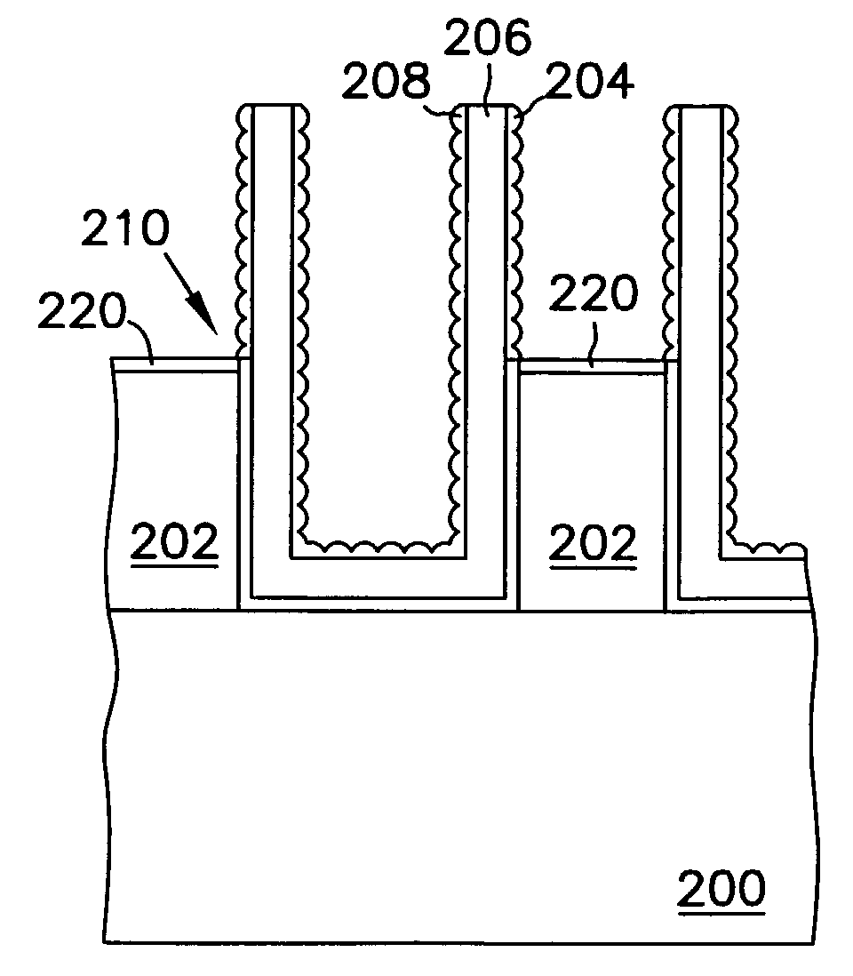
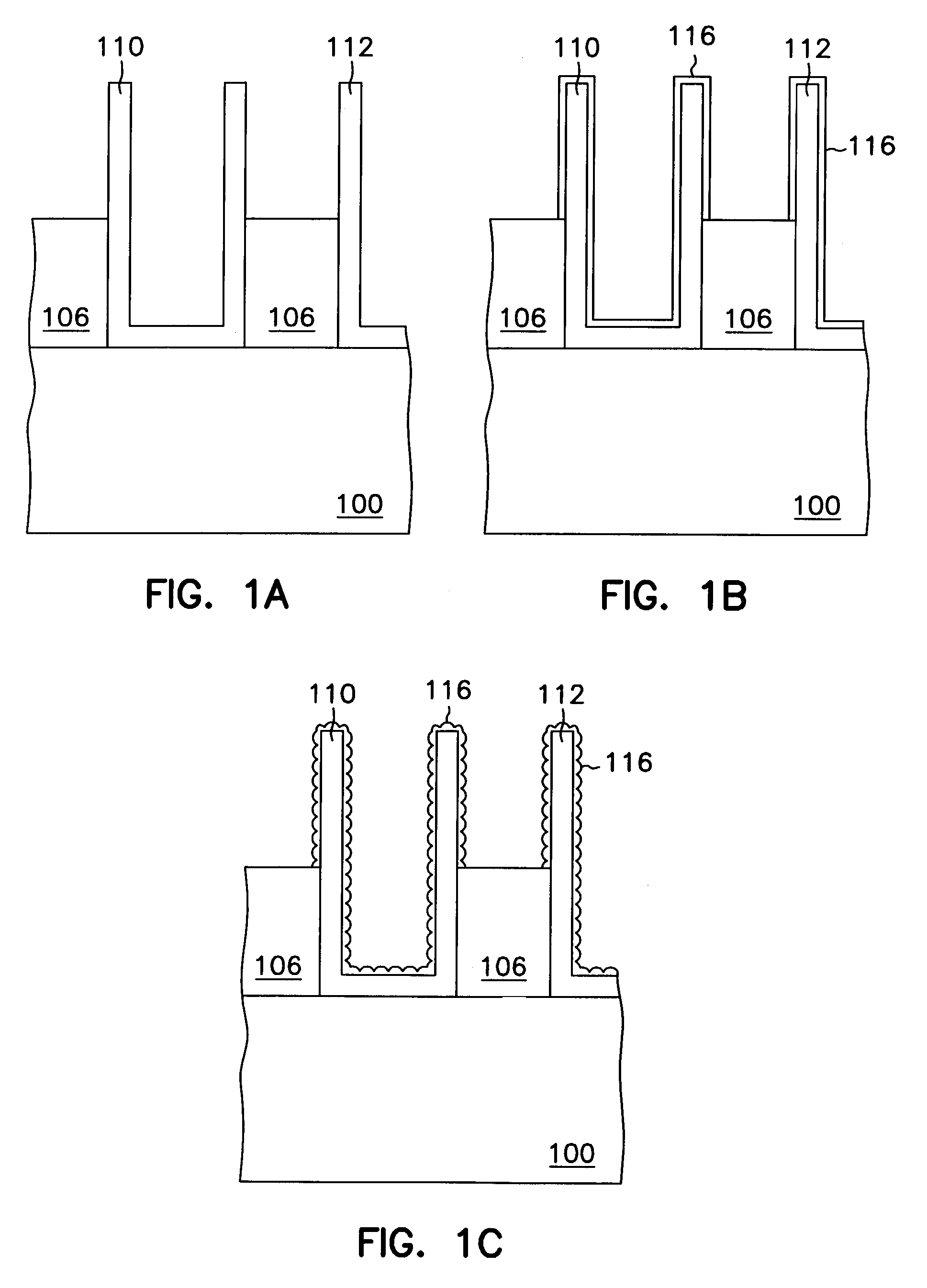
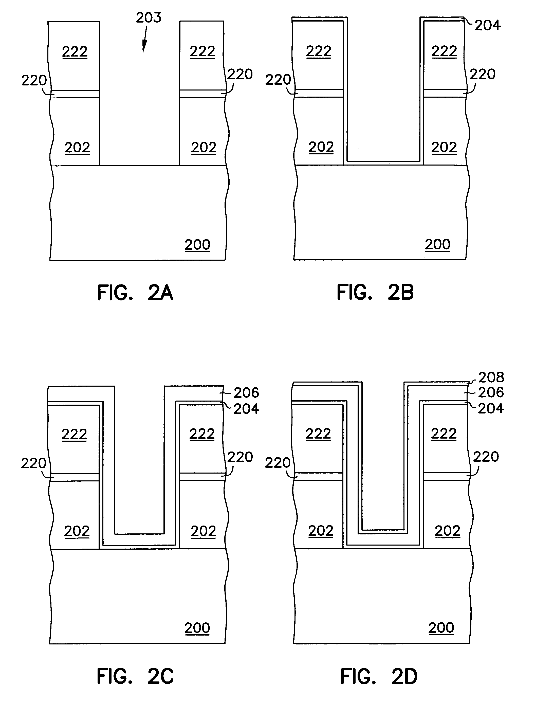
[0019]In the following detailed description, reference is made to the accompanying drawings which form a part hereof, and in which is shown by way of illustration specific embodiments in which the invention may be practiced. These embodiments are described in sufficient detail to enable those skilled in the art to practice the invention, and it is to be understood that other embodiments may be utilized and that structural, logical and electrical changes may be made without departing from the spirit and scope of the present invention. The following detailed description is, therefore, not to be taken in a limiting sense, and the scope of the present invention is defined by the appended claims. Numbering in the Figures is usually done with the hundreds and thousands digits corresponding to the figure number, with the exception that the same components may appear in multiple figures. Scaling in the Figures does not represent precise dimensions of the structures illustrated.

[0020]Wafer a...


PUM

PropertyMeasurementUnit
temperatureaaaaaaaaaa

Abstract

A polysilicon film is formed with enhanced selectivity by flowing chlorine during the formation of the film. The chlorine acts as an etchant to insulative areas adjacent polysilicon structures on which the film is desired to be formed. Bottom electrodes for capacitors are formed using this process, followed by an anneal to create hemishperical grain (HSG) polysilicon. Multilayer capacitor containers are formed in a non-oxidizing ambient so that no oxide is formed between the layers. The structure formed is planarized to form separate containers made from doped and undoped amorphous silicon layers. Selected ones of undoped layers are seeded in a chlorine containing environment and annealed to form HSG. A dielectric layer and second electrode are formed to complete the cell capacitor.

Description

RELATED APPLICATIONS[0001]This application is a Divisional of U.S. application Ser. No. 09 / 653,086 filed on Aug. 31, 2000, now issued as U.S. Pat. No. 6,521,507, which is a Continuation of U.S. Ser. No. 08 / 914,975, filed on Aug. 20, 1997, now issued as U.S. Pat. No. 6,146,967 on Nov. 14, 2000. These applications are incorporated herein by reference.FIELD OF THE INVENTION[0002]The present invention relates to semiconductor field effect transistors, and in particular to selective depostion on polysilicon surfaces.BACKGROUND OF THE INVENTION[0003]Dynamic random access memories (DRAMs) are a widely used form of semiconductor memory. DRAMs are composed of a memory cell array and peripheral circuitry. Each memory cell array is formed of a plurality of memory cells for storing information. Typical memory cells are formed with a transistor for accessing a capacitor that stores charge. Of primary concern is maximizing the storage capacitance of each memory cell capacitor. This need is partic...

Claims


Application Information

Patent Timeline
Patent Type & Authority Patents(United States)
IPC IPC(8): H01L21/20H01L21/02
CPCC23C16/045C23C16/24C23C16/56H01L27/10852H01L28/84H01L21/02664H01L21/0245H01L21/02505H01L21/02532H01L21/0262H01L28/91H01L28/90Y10S438/964H10B12/033
Inventor THAKUR, RANDHIR P. S.PAN, JAMES
Owner MICRON TECH INC
Why Eureka
Try Eureka