Compound semiconductor light-emitting diode

Inactive Publication Date: 2007-07-19
SHOWA DENKO KK
View PDF15 Cites 3 Cited by
  • Summary
  • Abstract
  • Description
  • Claims
  • Application Information

AI Technical Summary

Benefits of technology

[0020] The present invention has been conceived in an attempt to solve the aforementioned problems involved in the conventional techniques. Thus, the present invention provides a compound semiconductor LED exhibiting excellent electric characteristics including forward voltage through provision of a current diffusion laye

Problems solved by technology

Although a carrier-confining effect is attained, such a cladding layer is generally insufficient for diffusing a current for operating a device (i.e., device operation current) over a wide range of the light-emitting layer, since the cladding layer is formed from a semiconductor layer exhibiting a wide bandgap.
Therefore, even though the light-emitting layer has a heterojunction structure for attaining high-intensity light emission, high-intensity LEDs cannot be consistently and reliably produced so long as the LEDs have a conventional configuration in which a current diffusion layer is provided on the light-emitting area on the light extraction side.
However, transparent oxide generally encounters difficulty in consistently maintaining Ohmic contact with a Group III-V compound semiconductor, and diffusion of device operation current over a wide area may fail to be attained.
However, when the O

Method used


Image

  • Compound semiconductor light-emitting diode
  • Compound semiconductor light-emitting diode

Examples


example 1

[0099] The present invention will next be described in detail with reference to an exemplary boron phosphide LED having a current diffusion layer composed of a boron monophosphide semiconductor.

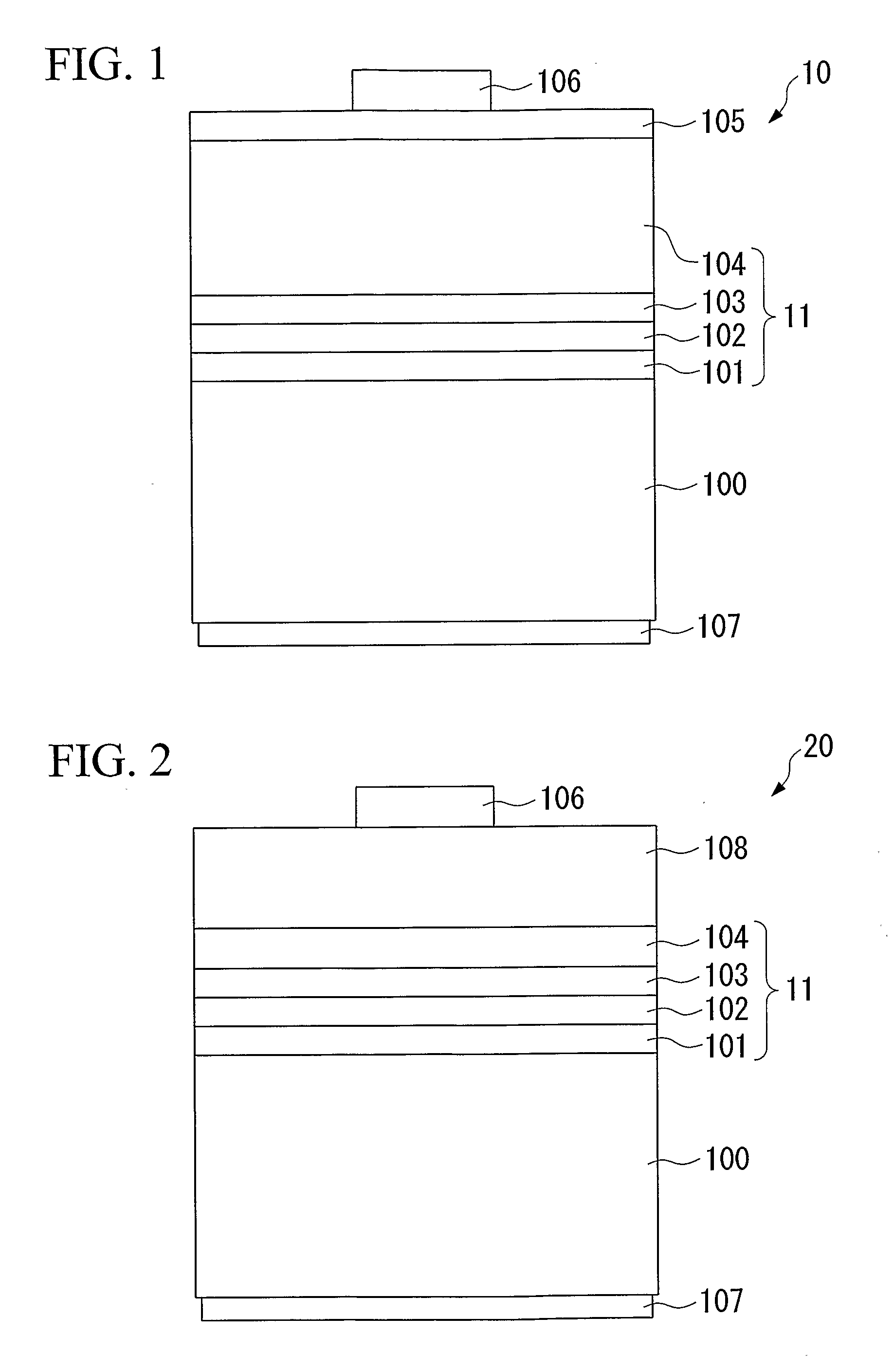
[0100]FIG. 1 is a schematic cross-sectional view of a boron phosphide LED 10 of Example 1 having a double-hetero (DH) junction structure and a stacked structure 11 thereof. Since FIG. 1 is a schematic view, dimensions (e.g., thickness proportions) of the component layers may be different from the actual values.

[0101] The stacked structure 11 was formed through sequentially stacking on a zinc (Zn)-doped p-type (100)-gallium arsenide (GaAs) single-crystal substrate 100 the following layers: a zinc-doped p-type GaAs buffer layer 101, a lower cladding layer 102 composed of a zinc-doped aluminum gallium indium phosphide mixed crystal ((Al0.70Ga0.30)0.50In0.50P), an undoped n-type light-emitting layer 103 composed of (Al0.14Ga0.86)0.50In0.50P, and a selenium (Se)-doped n-type upper cladding layer...

example 2

[0120] The present invention will next be described in detail with reference to an exemplary boron phosphide semiconductor LED having a boron-phosphide-based semiconductor layer (composition-graded layer) having a boron compositional gradient, the layer serving as both a current diffusion layer and a cladding layer.

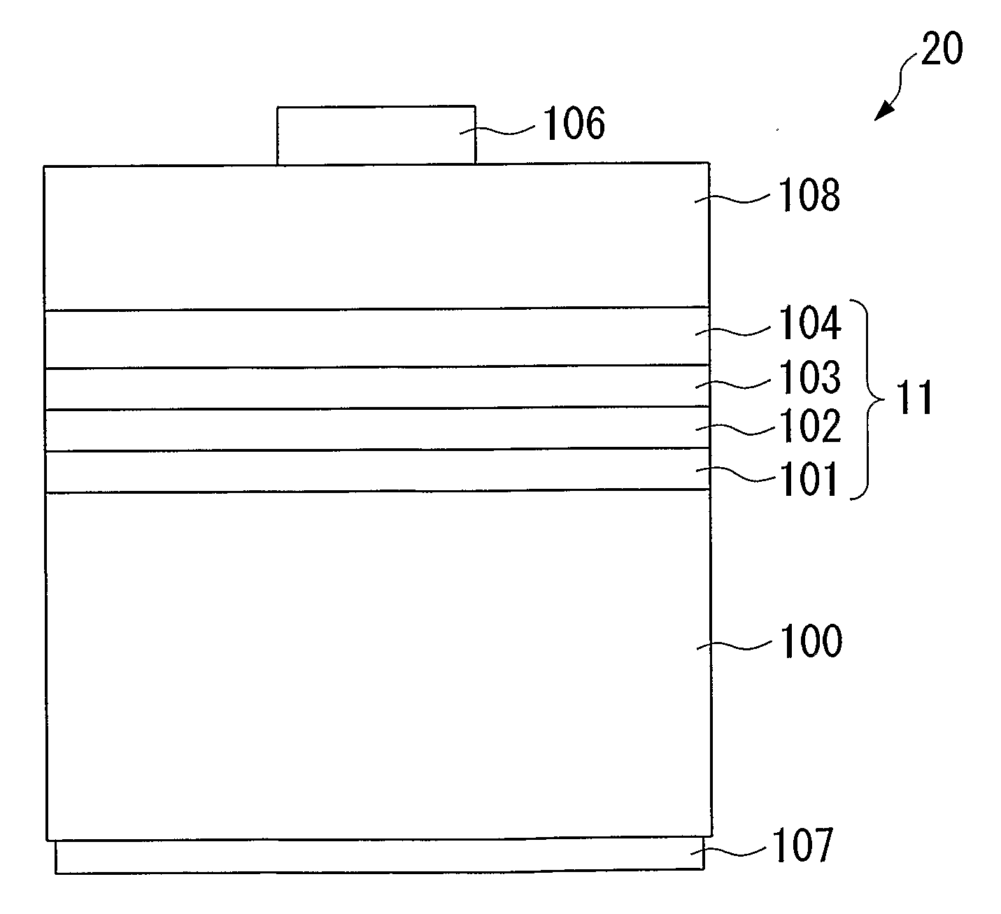
[0121]FIG. 2 is a schematic cross-sectional view of a boron phosphide LED 20 of Example 2. Similar to FIG. 1, since FIG. 2 is a schematic view, dimensions (e.g., thickness proportions) of the component layers may be different from the actual values.

[0122] The same members as employed in the boron phosphide LED 10 shown in FIG. 1 are denoted by the same reference numerals, and detailed description therefor is omitted.

[0123] In Example 2, a selenium (Se)-doped n-type upper cladding layer 104 employed in the boron phosphide LED 10 of Example 1 and composed of (Al0.70Ga0.30)0.50In0.50P was provided as a thin-film cladding layer (hereinafter the layer is also denoted by the...


PUM


Abstract

A compound semiconductor light-emitting diode comprising a light-emitting layer composed of a Group III-V compound semiconductor, and a current diffusion layer provided on the light-emitting layer and composed of a Group III-V compound semiconductor, characterized in that the current diffusion layer is composed of a conductive boron-phosphide-based semiconductor and has a bandgap at room temperature wider than that of the light-emitting layer.

Description

CROSS-REFERENCE TO RELATED APPLICATION [0001] This application claims the benefit pursuant to 35 U.S.C. §119(e)(1) of U.S. Provisional Application, No. 60 / 555,417 filed Mar. 23, 2004.TECHNICAL FIELD [0002] The present invention relates to a compound semiconductor light-emitting diode (hereinafter may be referred to as compound semiconductor LED) having a Group III-V compound semiconductor layer serving as a light-emitting layer, wherein the LED has a current diffusion layer for diffusing LED operation current over a wide area of the light-emitting layer, leading to high emission intensity. BACKGROUND ART [0003] LEDs having a light-emitting layer composed of an aluminum gallium indium phosphide mixed crystal (compositional formula: AlXGaYInZP: 0≦X, Y, Z≦1, X+Y+Z=1) are known to emit light having a wavelength corresponding to green light to red light (see Y. Hosokawa et al., J. Crystal Growth, Vol. 221 (2000), Holland, p. 652-656). [0004] As disclosed in aforementioned Y. Hosokawa et ...

Claims


Application Information

Patent Timeline
IPC IPC(8): H01L33/00H01L33/14H01L33/30
CPCH01L21/02395H01L21/02463H01L21/02543H01L33/30H01L21/0262H01L33/14H01L21/02573
Inventor TAKEUCHI, RYOUICHIUDAGAWA, TAKASHI
Owner SHOWA DENKO KK
Why Eureka
Try Eureka