Substrate for thin-film solar cell, method for producing the same, and thin-film solar cell employing it

a technology substrates, which is applied in the direction of photovoltaics, electrical devices, semiconductor devices, etc., can solve the problems of reducing the formation temperature of the transparent electrode layer and the formation temperature of the silicon based semiconductor layer, and the inability to obtain effective “light trapping” effect so as to achieve efficient light trapping effect, improve the performance of thin film solar cells, and increase the uneven effect of substrates

Inactive Publication Date: 2007-07-26
KANEKA CORP
View PDF2 Cites 59 Cited by
  • Summary
  • Abstract
  • Description
  • Claims
  • Application Information

AI Technical Summary

Benefits of technology

[0019] An object of the present invention is to effectively increase unevenness of a substrate for thin film solar cells, and to acquire efficient light trapping effect, to provide inexpensive substrates for thin film solar cel...

Problems solved by technology

First, as shown in FIG. 1, in the case where ZnO is formed on a base material without foundation layer as in prior art 1, it is difficult to make a haze ratio higher, for example, up to not less than 20%, resulting in failure of obtaining effective “light trapping.” Since film-formation of a transparent electrode layer at base material temperatures of not less than 150 degrees C. reduces a haze ratio especially when not using foundation layer, the conventional method of prior art 1 leads to a problem of decrease in a short circuit current density of the thin film solar cell.
Generally, a larger difference between a formation temperature of the transparent electrode layer and that of the silicon based semiconductor layer tends to give more serious heat damage to the transparent electrode layer.
Therefore, the technique of prior art 1 has problems of decrease in...

Method used


Image

  • Substrate for thin-film solar cell, method for producing the same, and thin-film solar cell employing it
  • Substrate for thin-film solar cell, method for producing the same, and thin-film solar cell employing it
  • Substrate for thin-film solar cell, method for producing the same, and thin-film solar cell employing it

Examples


example 1

[0097] A thin film solar cell 5 as shown in FIG. 6 was produced as Example 1.

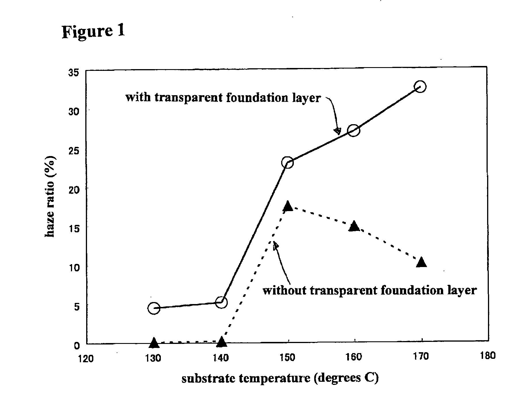
[0098] A glass substrate of 0.7 mm in thickness and measuring 125 mm per side was used as a transparent base material 111, and a transparent foundation layer 112 including SiO2 micro-particles 1121 was formed on the glass substrate. A coating liquid used for forming a transparent foundation layer 112 was obtained in a manner that tetra-ethoxy silane was added to a mixed liquor of dispersion liquid of a spherical silica having a particle diameter of 50 nm, water, and ethyl cellosolve, and then hydrochloric acid was further added to hydrolyze the silica. After applying the coating liquid on the glass substrate 111 with a printing machine, the substrate was dried at 90 degrees C. for 30 minutes, and then heated at 350 degrees C. for 5 minutes to obtain a transparent insulating substrate 11 having fine unevenness formed on a surface thereof. When a surface of this transparent insulating substrate 11 was observ...

example 2

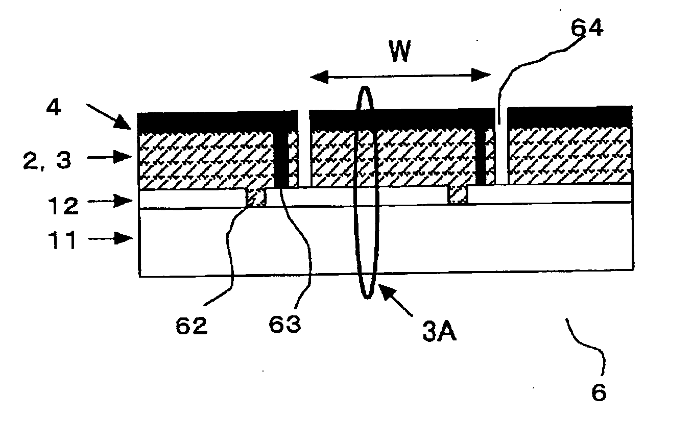
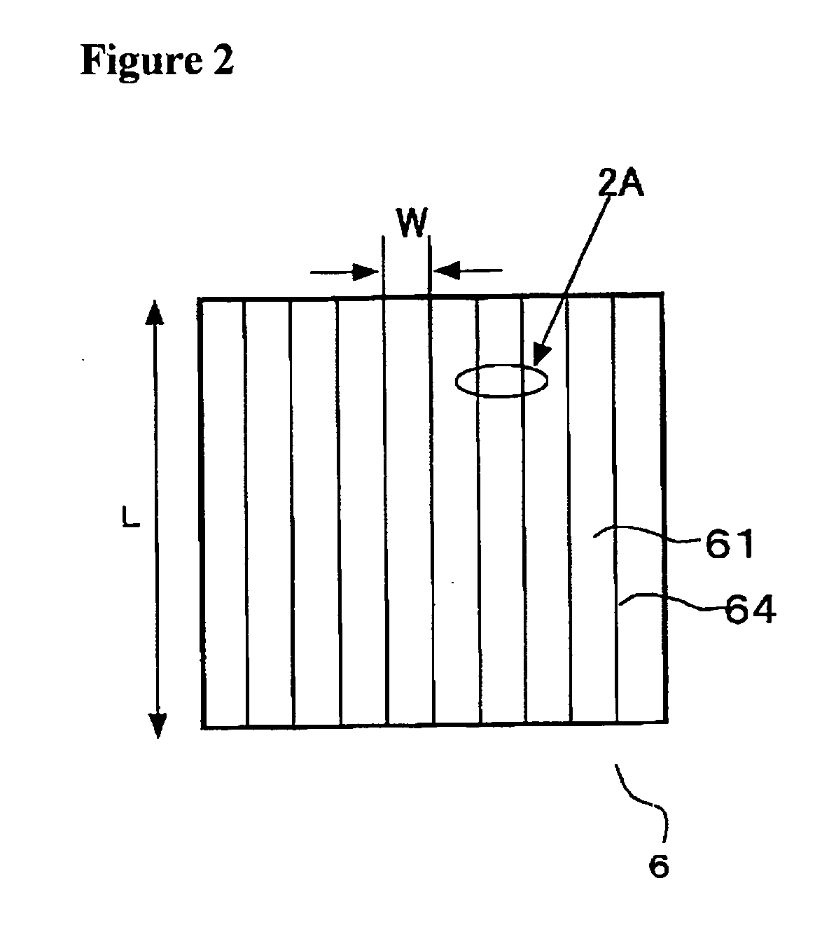
[0106] Also in Example 2, an integrated type crystalline silicon based thin film solar cell 6 was produced in a same manner as in Example 1, except for having used a substrate having an area of 910 mm×455 mm and a thickness of 4 mm as a glass substrate 111. An RMS of the transparent foundation layer 112 thus formed on this condition gave 9.8 nm.

[0107] Although ultrasonic cleaning was given after laser scribe process of a back electrode layer isolation groove 64, a film peeling area on the substrate was not identified. A number of stages of the cell connected in series after integration gave 48 stages.

[0108] By irradiating light of AM1.5 with a quantity of light of 100 mW / cm2, thus obtained integrated type silicon based thin film solar cell 6 was measured for an output characteristic. An open circuit voltage (Voc) per one step gave 0.541 V, a Jsc 23.6 mA / cm2, an F. F. 71.7%, and a conversion efficiency 9.2%.

[0109] A conversion efficiency was maintained although the integrated type...

example 3

[0110] In Example 3, an integrated type silicon based thin film solar cell 6 was produced almost in a same manner as in Example 2, except for having intentionally set the RMS greater using SiO2 micro-particles 1121 having a particle diameter of 80 nm in formation of the transparent foundation layer 112. An RMS of the transparent foundation layer 112 thus formed on this condition gave 19.3 nm. Although ultrasonic cleaning was given after laser scribe process of a back electrode layer isolation groove 64, a film peeling area on the substrate was not identified.

[0111] By irradiating light of AM1.5 with a quantity of light of 100 mW / cm2, thus obtained integrated type silicon based thin film solar cell 6 was measured for an output characteristic. An open circuit voltage (Voc) per one step gave 0.532 V, a Jsc 24.3 mA / cm2, an F. F. 70.5%, and a conversion efficiency 9.1%.


PUM


Abstract

An inexpensive substrate for thin film solar cells having improved performance of a thin film solar cell, and a manufacturing method thereof are provided by increasing light trapping effect due to effective increase in unevenness of a substrate for thin film solar cells. Furthermore, a thin film solar cell having improved performance using the substrate is provided. A substrate for thin film solar cells of the present invention has a transparent insulating substrate and a transparent electrode layer deposited thereon including at least zinc oxide (ZnO), the transparent insulating substrate has a fine surface unevenness having a root-mean-square deviation of the surface (RMS) 5 to 50 nm in an interface by a side of the transparent electrode layer, a projected area thereof consists of a curved surface, and furthermore a haze ratio or a ratio of a diffuse transmittance to a total transmittance as an index of unevenness of a substrate may be set at not less than 20% measured using a C light source. And thereby light trapping effect may effectively occur to improve performance of the thin film solar cell.

Description

TECHNICAL FIELD [0001] The present invention relates to a substrate for thin film solar cells, a method for manufacturing the same, and thin film solar cells therewith. BACKGROUND ART [0002] In recent years, for coexistence of cost reduction and higher efficiency of solar cells, thin film solar cells consuming only a small amount of raw materials attract attention, and wholehearted development is now being performed. Especially, expected is, as a method for enabling cost reduction, a method for forming an excellent semiconductor layer on an inexpensive transparent base material, such as glass, using a low-temperature process. [0003] When such a thin film solar cell is manufactured as a thin film solar cell having a large area enabling generation of electric power with a high output at a high voltage, generally used is a method wherein a plurality of thin film solar cells formed on a substrate with a large area connected in series are not used, but in order to obtain excellent yield,...

Claims


Application Information

Patent Timeline
IPC IPC(8): H01L31/00H01L31/0224H01L31/0236H01L31/0392
CPCH01L31/022466Y02E10/50H01L31/03921H01L31/0236H01L31/022483H01L31/02366H01L31/1884H01L31/02363
Inventor SASAKI, TOSHIAKIKOI, YOHEITAWADA, YUKOYAMAMOTO, KENJI
Owner KANEKA CORP
Why Eureka
Try Eureka