Flip-chip light emitting diode with high light-emitting efficiency

a light-emitting diode and flip-chip technology, applied in the direction of semiconductor devices, semiconductor/solid-state device details, electrical devices, etc., can solve the problem of not being able to efficiently emit light, and achieve the effect of reducing the thermal conductive distance of leds, high light-emitting efficiency, and prolonging the life of components

Inactive Publication Date: 2007-07-26
FORMOSA EPITAXY INCORPORATION
View PDF4 Cites 31 Cited by
  • Summary
  • Abstract
  • Description
  • Claims
  • Application Information

AI Technical Summary

Benefits of technology

[0006] Therefore it is a primary object of the present invention to provide a light emitting diode that is a flip-chip light emitting diode with high light-emitting efficiency so that the light from the light-emitting layer is reflected for preventing the light from being shielded.
[0007] It is another object of the present invention to provide a light emitting diode that the LED chip is disposed in a face-down orientation to the conductive substrate by the flip-chip technology so as to decrease thermal conductive distance of the LED, extend lifetime of the component, and further decrease the package volume.
[0008] In order to achieve above objects, a flip-chip light emitting diode with high light-emitting efficiency in accordance with the present invention includes a transparent conductive layer, an oxide layer, a reflective metal layer, a conductive layer, and a protective diffusion layer sequentially disposed over a p-type semiconductor layer so ass to reflect light from a light-emitting layer for enhancing light-emitting efficiency of the LED. Moreover, the present invention disposes the LED chip in a face-down orientation on a conductive substrate by flip-chip technology so as to enhance heat-dissipation efficiency of the LED. Further the lifetime of the LED is extended.

Problems solved by technology

Thus such kind of LED still can't emit light efficiently.

Method used


Image

  • Flip-chip light emitting diode with high light-emitting efficiency
  • Flip-chip light emitting diode with high light-emitting efficiency
  • Flip-chip light emitting diode with high light-emitting efficiency

Examples


Embodiment Construction

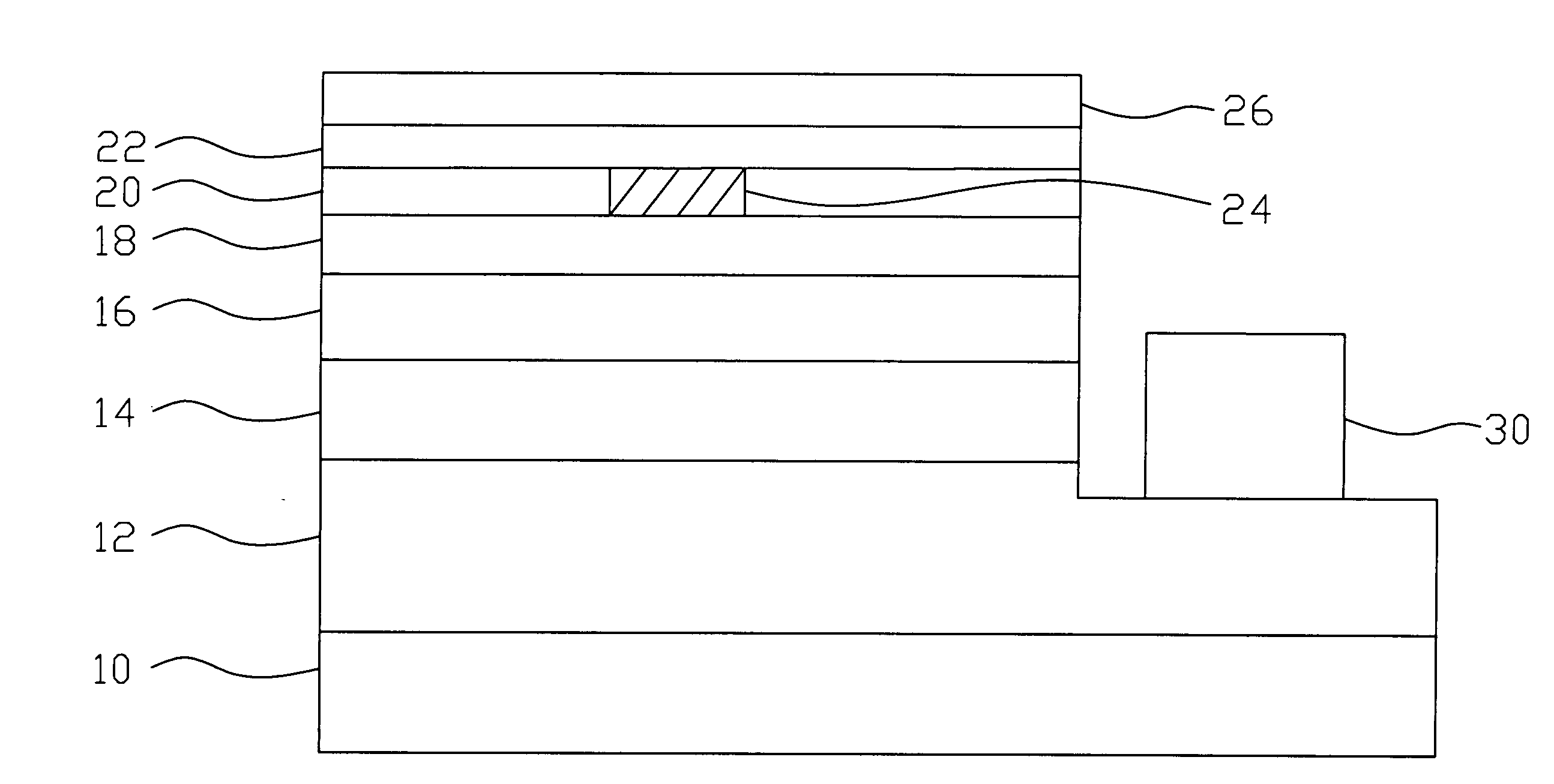
[0014] Refer to FIG. 3, a LED chip in accordance with the present invention is composed by a transparent substrate 10, a semiconductor stacked layer, a transparent conductive layer 18, an oxide layer 20, a reflective metal layer 22, a conductive layer 24, a protective diffusion layer 26 and a first electrode 30. The transparent substrate 10 is made from one of the following material: sapphire, silicon carbide (SiC), zinc oxide (ZnO), gallium phosphide (GaP), gallium arsenide (GaAs), or other material with high transparency.

[0015] Moreover, the semiconductor stacked layer, arranged over the transparent substrate 10, having a n-type semiconductor layer 12, a light emitting layer 14 and a p-type semiconductor layer 16 while the light emitting layer 14 is located between the n-type semiconductor layer 12 and the p-type semiconductor layer 16. The n-type semiconductor layer 12 is a n-GaN layer and the p-type semiconductor layer 16 is a p-GaN layer.

[0016] The light emitting layer 14 is ...


PUM


Abstract

A flip-chip light emitting diode with high light-emitting efficiency is disclosed. The LED includes a transparent conductive layer, an oxide layer, a reflective metal layer, a conductive layer, and a protective diffusion layer sequentially disposed over a p-type semiconductor layer. Thereby, light emitting from a light-emitting layer toward the p-type semiconductor layer is reflected and penetrating a transparent substrate and emitting outwards. Thus the problem of light shielded from the flip-chip type LED is solved and the light-emitting efficiency is improved. Furthermore, the present invention disposes the LED chip in a face-down orientation on a conductive substrate by flip-chip technology so as to enhance heat-dissipation efficiency of the LED.

Description

BACKGROUND OF THE INVENTION [0001] The present invention relates to a light emitting diode, especially to a flip-chip light emitting diode with high light-emitting efficiency. [0002] Due to large power consumption of conventional illumination devices caused by high power, people in industry or research institute in various countries are dedicated to developing illuminative components and the related design. Thus the light emitting diode (LED) is invented. [0003] Refer to FIG. 1, it is a schematic drawing of conventional Light-emitting gallium nitride-based III-V group compound semiconductor device consisting of a gallium nitride buffer layer 2′, a n-type gallium nitride ohmic contact layer 3′, an indium gallium nitride (InGaN) emitting layer 4′, a p-type p-type aluminum gallium nitride cladding layer 5′, a p-type gallium nitride ohmic contact layer 6′ and a p-type transparent conductive metal layer 7′ in sequence. The epitaxy is growing on a sapphire substrate 1′. A positive electro...

Claims


Application Information

Patent Timeline
Patent Type & Authority Applications(United States)
IPC IPC(8): H01L23/52
CPCH01L33/32H01L33/405H01L2924/3025H01L33/42H01L33/62H01L2224/48091H01L2224/49107H01L2924/01004H01L2924/01012H01L2924/01029H01L2924/01046H01L2924/01077H01L2924/01078H01L2924/01079H01L2924/04941H01L2924/00014
Inventor WEN, WAY-JZELIN, YI-FONGPAN, SHYI-MINGCHIEN, FEN
Owner FORMOSA EPITAXY INCORPORATION
Why Eureka
Try Eureka