Tungsten based sintered compact and method for production thereof
- Summary
- Abstract
- Description
- Claims
- Application Information
AI Technical Summary
Benefits of technology
Problems solved by technology
Method used
Image
Examples
example 1
[0110] Example 1 is one example of a discharge lamp electrode formed of the tungsten-based sintered body of the present invention.
[0111] A tungsten powder having a purity of 99.99% and an average particle size of 0.8μ was used as a starting material.
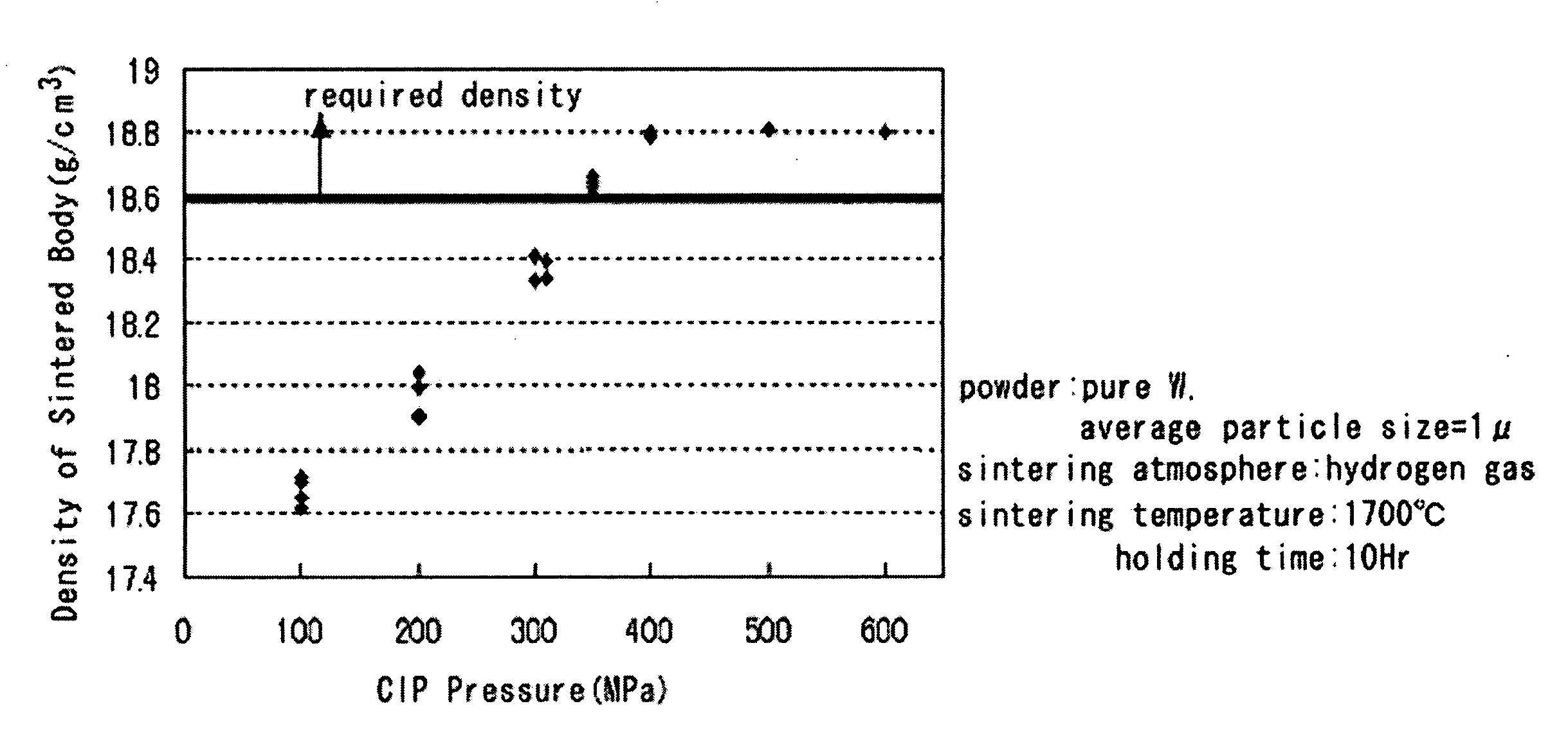
[0112] The powder was subjected to die pressing at a pressure of 2 MPa to form a cylindrical-shaped preform of φ 100×250. This preform was put in a hermetically-closable rubber bag and subjected to a CIP process at a pressure of 400 MPa.
[0113] A powder compact after the CIP process had a size of φ 80×200 and a density of about 11 g / cm3.
[0114] This powder compact was formed in a discharge-lamp-electrode shape having a cylindrical column with a hemispherical head, using a lathe.
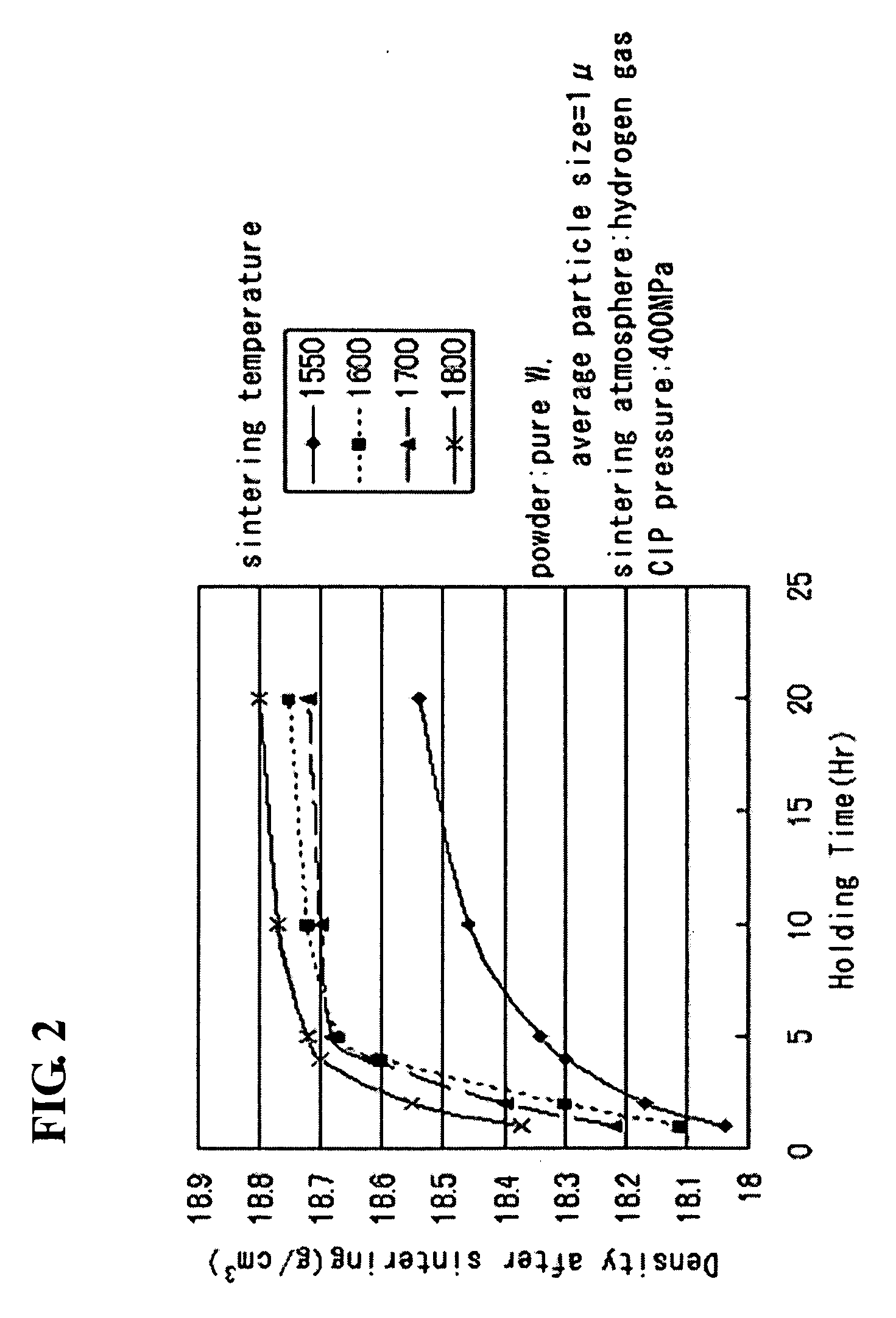
[0115] The machined powder compact was sintered in a hydrogen gas atmosphere at a temperature of 1800° C. for a holding time of 6 hours. The powder compact was heated to 1000° C. at a heating rate of 10° C. / min and then heated to 1800° C. at a heating rate of 4...
example 2
[0121] In the same manner as Example 1 except for the raw powder and a shape of the sintered body, a sputtering target, a crucible, a radiation shielding member, a resistance welding electrode, a semiconductor element mounting substrate and a switch contact were produced. Table 4 shows their advantages in performance and cost, based on the sintered body of the present invention.
TABLE 4ProductComparative ProductFeatureAdvantageSputtering TargetTungsten sputtering target with aSmall number of poresPrevention of uneven wearingdensity of less than 99.5%Low contaminationHigh purityLow contaminationUniform structurePrevention of uneven wearingCrucibleTungsten crucible with a densitySmall number of poresLow contaminationof less than 99.5%Intermediate working OKLow production costRadiation ShieldingTungsten shielding plateHigh densityHigh shielding effectMemberobtained through a forgingIntermediate working OKLow production costprocessResistance WeldingTungsten chip for a resistanceSmall n...
PUM
| Property | Measurement | Unit |
|---|---|---|
| Temperature | aaaaa | aaaaa |
| Temperature | aaaaa | aaaaa |
| Length | aaaaa | aaaaa |
Abstract
Description
Claims
Application Information


