Heterostructure including light generating structure contained in potential well

a technology of heterostructure and potential well, applied in the field of heterostructure, can solve the problems of affecting the performance of nitride-based light emitting diodes and lasers, the relatively poor efficiency with which light is generated by the light generating structure is a significant barrier to improving the performance of the device, and the efficiency is limited, so as to achieve the effect of improving one or more of their characteristics

Active Publication Date: 2007-08-09
SENSOR ELECTRONICS TECH
View PDF5 Cites 85 Cited by
  • Summary
  • Abstract
  • Description
  • Claims
  • Application Information

AI Technical Summary

Benefits of technology

[0011]The invention provides an improved nitride-based light emitting heterostructure. The nitride-based light emitting heterostructure includes an electron supply layer and a hole supply layer with a light generating structure disposed there between. The light generating structure includes a set of barrier layers, each of which has a graded composition, and a set of quantum wells, each of which adjoins at least one barrier layer. Additional features, such as a thickness of each qua

Problems solved by technology

However, to date, the performance of nitride-based light emitting diodes and lasers quickly worsens as the radiation wavelength is reduced into the ultraviolet range.
The relatively poor efficiency with which light is generated by the light generating structure is a significant barrier to improving the performance of the device in generating light having the shorter wavelengths.
Such efficiency is limited by a large difference between the mobilities of electrons and holes.
However, these approaches still fail to provide a solution that efficiently g

Method used


Image

  • Heterostructure including light generating structure contained in potential well
  • Heterostructure including light generating structure contained in potential well
  • Heterostructure including light generating structure contained in potential well

Examples


Embodiment Construction

[0033]It is understood that for the purposes of the present disclosure, Al means Aluminum, Be means Beryllium, C means Carbon, Ga means Gallium, In means Indium, Li means Lithium, Mg means Magnesium, Mn means Manganese, N means Nitrogen, O means Oxygen, and Si means Silicon.

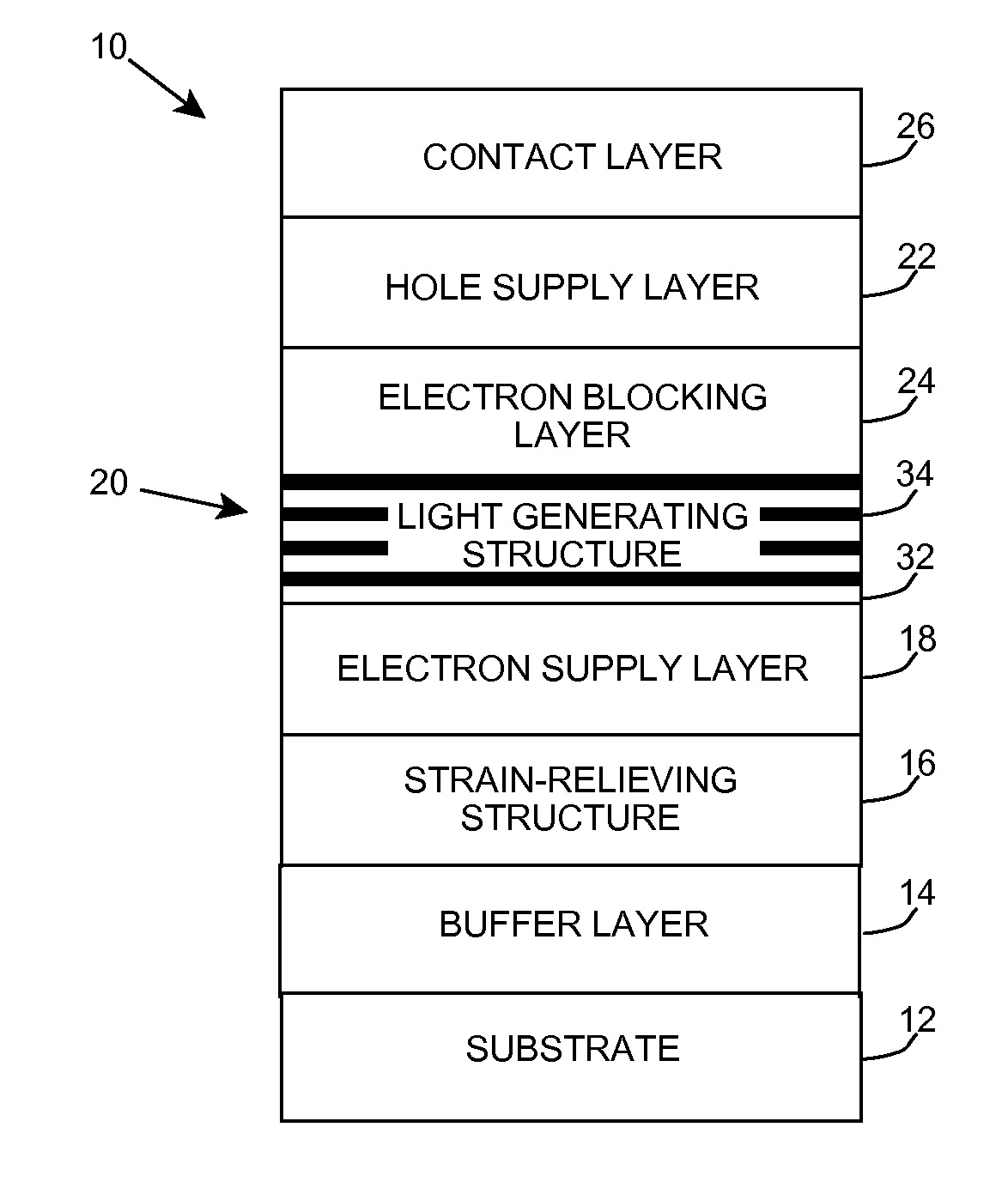
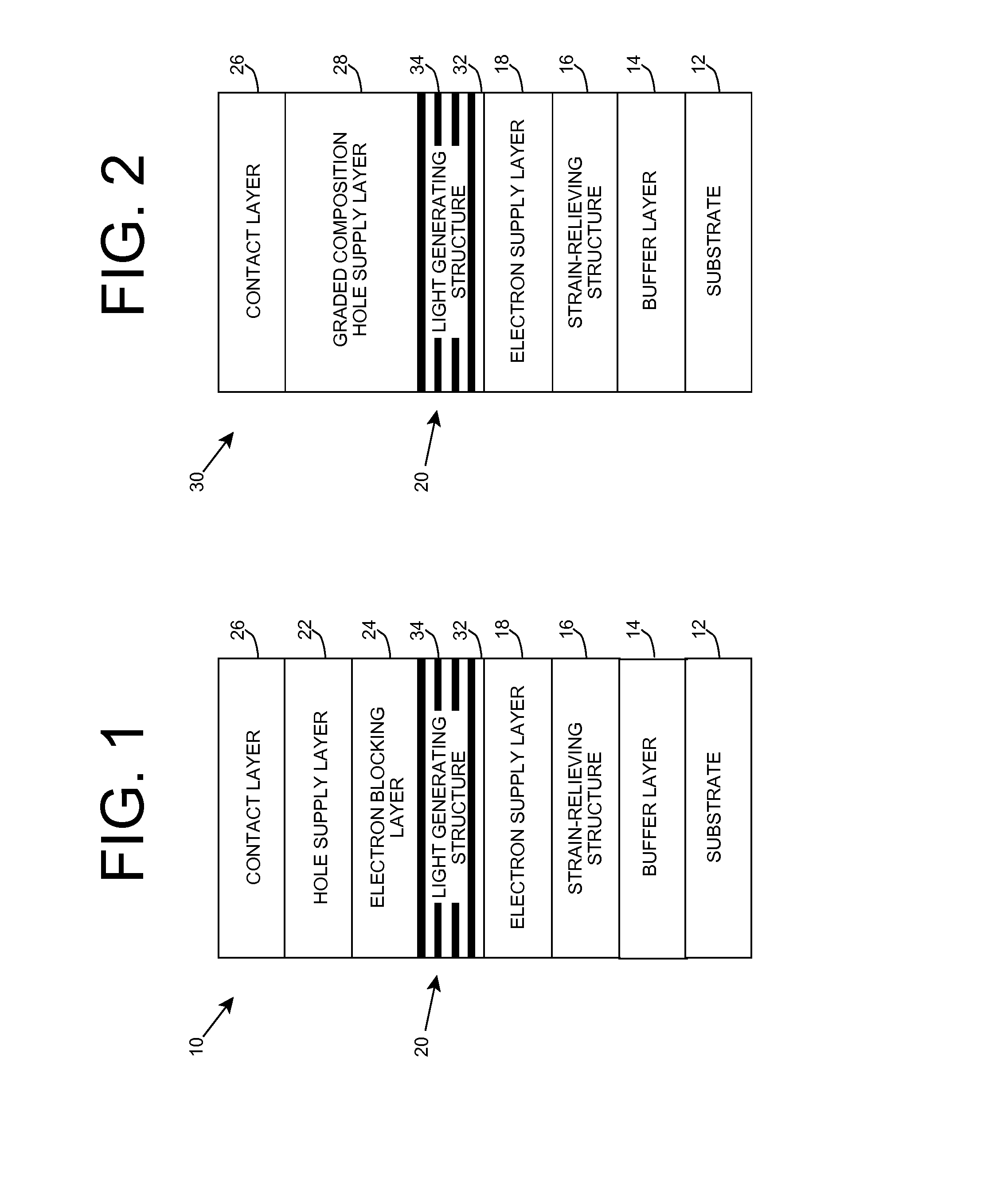
[0034]As indicated above, the invention provides an improved nitride-based light emitting heterostructure. The nitride-based light emitting heterostructure includes an electron supply layer and a hole supply layer with a light generating structure disposed there between. The light generating structure includes a set of barrier layers, each of which has a graded composition, and a set of quantum wells, each of which adjoins at least one barrier layer. Additional features, such as a thickness of each quantum well, can be selected / incorporated into the heterostructure to improve one or more of its characteristics. Further, one or more additional layers that include a graded composition can be included in the heteros...


PUM


Abstract

A light emitting heterostructure and/or device in which the light generating structure is contained within a potential well is provided. The potential well is configured to contain electrons, holes, and/or electron and hole pairs within the light generating structure. A phonon engineering approach can be used in which a band structure of the potential well and/or light generating structure is designed to facilitate the emission of polar optical phonons by electrons entering the light generating structure. To this extent, a difference between an energy at a top of the potential well and an energy of a quantum well in the light generating structure can be resonant with an energy of a polar optical phonon in the light generating structure material. The energy of the quantum well can comprise an energy at the top of the quantum well, an electron ground state energy, and/or the like.

Description

REFERENCE TO PRIOR APPLICATIONS[0001]The current application claims the benefit of co-pending U.S. Provisional Application No. 60 / 765,270, entitled “Light Emitting Heterostructure”, which was filed on 4 Feb. 2006, which is hereby incorporated herein by reference. Aspects of the current application also are related to the co-owned, co-pending U.S. patent application Ser. No. 11 / 292,519, entitled “Nitride-Based Light Emitting Heterostructure”, which was filed on 2 Dec. 2005, and which also is hereby incorporated herein by reference.FIELD OF THE INVENTION[0002]The invention relates generally to heterostructures, and more particularly, to an improved light emitting heterostructure.BACKGROUND OF THE INVENTION[0003]Recently, a great deal of interest is focused on nitride-based light emitting diodes and lasers that emit light in the blue and deep ultraviolet (UV) wavelengths. These devices may be capable of being incorporated into various applications, including solid-state lighting, bioch...

Claims


Application Information

Patent Timeline
IPC IPC(8): H01L31/00H01L21/00
CPCH01L33/06B82Y20/00
Inventor GASKA, REMIGIJUSSHUR, MICHAELZHANG, JIANPING
Owner SENSOR ELECTRONICS TECH
Why Eureka
Try Eureka