Organosilicate resin formulation for use in microelectronic devices

a technology of organic resin and microelectronic devices, which is applied in the direction of instruments, photomechanical devices, coatings, etc., to achieve the effects of increasing the need, increasing the light scattering, and increasing the uv light absorption

Active Publication Date: 2007-08-09
DOW GLOBAL TECH LLC
View PDF22 Cites 26 Cited by
  • Summary
  • Abstract
  • Description
  • Claims
  • Application Information

AI Technical Summary

Benefits of technology

[0032] According to yet another embodiment of the present invention, one or more of a composition according to the present invention are provided for purposes of absorbing light, especially UV light that is reflected or scattered during one or more subsequent exposure and / or curing steps during the preparation of printed circuits or other electronic devices. Such antireflective layers are especially beneficial when used in an immersion lithography process employing a fluid other than air, especially water, for transmission of the ultra-violet light. Such processes can produce increased light scatter and / or alter the angle of incidence thereby increasing the need for greater UV light absorption. In a particularly desirable embodiment, multiple layers, preferably 2, 3 or 4 layers, of the present composition, each differing slightly in light absorption properties (obtainable by adjustment of aromatic group content of the polymer) can be deposited and cured in order to give maximal UV absorption properties to the composite structure.

Problems solved by technology

Due to the latent acid catalyst, the composition may be shipped, stored and applied under conditions that would previously lead to premature curing.

Method used


Image

  • Organosilicate resin formulation for use in microelectronic devices
  • Organosilicate resin formulation for use in microelectronic devices
  • Organosilicate resin formulation for use in microelectronic devices

Examples


example 1

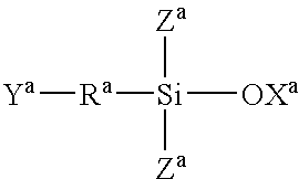
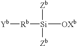
[0123] A) Synthesis of 90 / 10 Mole Percent Vinyl / Phenyl Organosilicate

[0124] A 250 ml, 3 neck round bottom flask is placed in a 20° C. water bath and fitted with a stirrer connected to an air motor, a water jacketed condenser, a thermocouple connected to a temperature controller, and an addition funnel. 21.6 Grams (1.2 moles) of acidified water (3N acetic acid) is added to the flask. 53.3 Grams (0.360 moles) of vinyltrimethoxysilane and 7.94 grams (0.040 moles) of phenyltrimethoxysilane are pre-mixed and added to the addition funnel. The silanes are added to the reactor over 45 minutes. After the addition is complete the water bath is removed and a heating mantle placed under the flask. The addition funnel is removed and a dean-stark trap and a nitrogen sweep line are attached. The solution is slowly heated to 100° C. While heating, methanol and acetic acid are collected in the trap. When the reaction reached 100° C., 100 grams of propyleneglycol monomethylether acetate are added. T...

example 2

[0128] Photo hard mask compositions for imaging are prepared by adding 8 percent (based on resin solids) of a cationic photoacid generator comprising mixed triarylsulfonium hexafluoroantimonate salts (CYRACURE® UVI-6976 available from The Dow Chemical Company) to representative organosilicate resins (100 percent vinyltrimethoxysilane or a mixture (95:5 mole:mole) of vinyltrimethoxysilane and phenyltrimethoxysilane). Compositions are diluted to 15 percent solids using propylene glycol methyl ether acetate solvent (Dowanol™ PMA from The Dow Chemical Company) and then filtered through 0.22 μm PTFE filters. Approximately 2 ml of the photo hard mask composition is dispensed (puddled) onto a static 4 inch (10 cm) silicon wafer. After dispensing, the wafer is initially spun at 500 RPM for 5 seconds, followed by a second spin cycle at 2000 or 5000 RPM for 30 seconds. After applying the photo hard mask composition, the coated silicon wafer is pre-exposure baked on a direct hotplate (Model VB...

example 3

[0130] 90:10 Vinyl:Phenyl Organosilicate Resin (MW=2120).

[0131] The reaction conditions of Example 2 are substantially repeated using a 90:10 mole:mole mixture of vinyltrimethoxysilane and phenyltrimethoxysilane resins. Samples included 8 percent CYRACURE® UVI-6976 and are spun at 500 RPM for 5 seconds, followed by a second spin cycle at 5000 RPM for 30 seconds, and then pre-exposure baked in an oven set at 55° C. for 60 seconds. After exposure, films are post-baked in an oven set at 180° C. for 60 seconds. Films are developed in 2.38 percent aqueous TMAH. Results are contained in Table 3.

TABLE 3RadiationSmallest Via thatDosage (mJ / cm2)completely opened (μm)50.03545.62530.92514.7156.715


PUM

PropertyMeasurementUnit
dielectric constantaaaaaaaaaa
temperaturesaaaaaaaaaa

Abstract

A curable organosilicate composition that is employed to form one or more layers in the fabrication of electronic devices comprising: (a) an alkoxy or acyloxy silane having at least one group containing ethylenic unsaturation which group is bonded to the silicon atom (b) an alkoxy oracyloxy silane having at least one group containing an aromatic ring which group is bonded to the silicon atom, (c) a latent acid catalyst, and (d) optionally an alkoxy or acyloxy silane having at least one C1-C6 alkyl group bonded to the silicon atom.

Description

BACKGROUND OF THE INVENTION [0001] This invention relates to the use of organosilicate resins as hardmasks, etchstops, antireflective layers, adhesion promotion layers, chemical / mechanical polishing (CMP) stop layers, or other layers and combinations of layers in the fabrication of microelectronic devices, to a method of fabricating such devices, and to the resulting electronic devices. [0002] The microelectronics fabrication industry is moving toward smaller geometries in its devices to enable lower power consumption and faster device speeds. As the conductor lines become finer and more closely packed, the requirements of the dielectrics between such conductors become more stringent. New materials having a lower dielectric constant than the dielectric constant for silicon dioxide, the traditionally used dielectric material, are being investigated. Among the lower dielectric materials that are attaining increased acceptance are spin-on, organic, inorganic or hybrid polymers having a...

Claims


Application Information

Patent Timeline
Patent Type & Authority Applications(United States)
IPC IPC(8): C08G77/12C09D183/04G03F7/004G03F7/075G03F7/09H01L21/312
CPCC09D4/00C09D183/04G03F7/0045G03F7/0755G03F7/0757G03F7/091H01L21/3122H01L21/02126H01L21/02216H01L21/02282C08G77/20
Inventor BAIKERIKAR, KIRAN K.FENG, SHAOGUANGHETZNER, JACK E.MAHER, JOHN M.MILLS, MICHAEL E.POPA, PAUL J.STRITTMATTER, RICHARD J.WILSON, LARRY R.
Owner DOW GLOBAL TECH LLC
Why Eureka
Try Eureka