

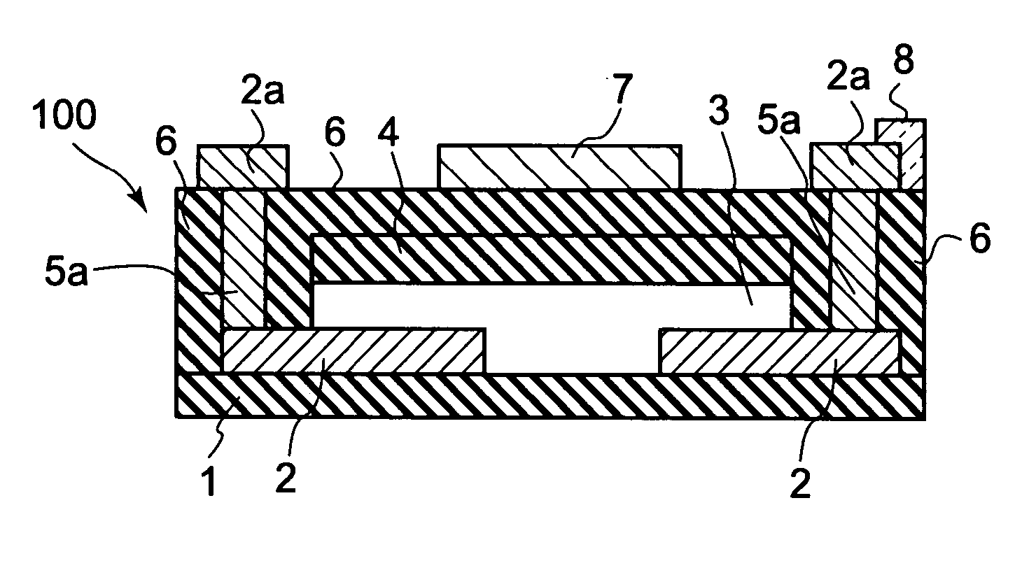
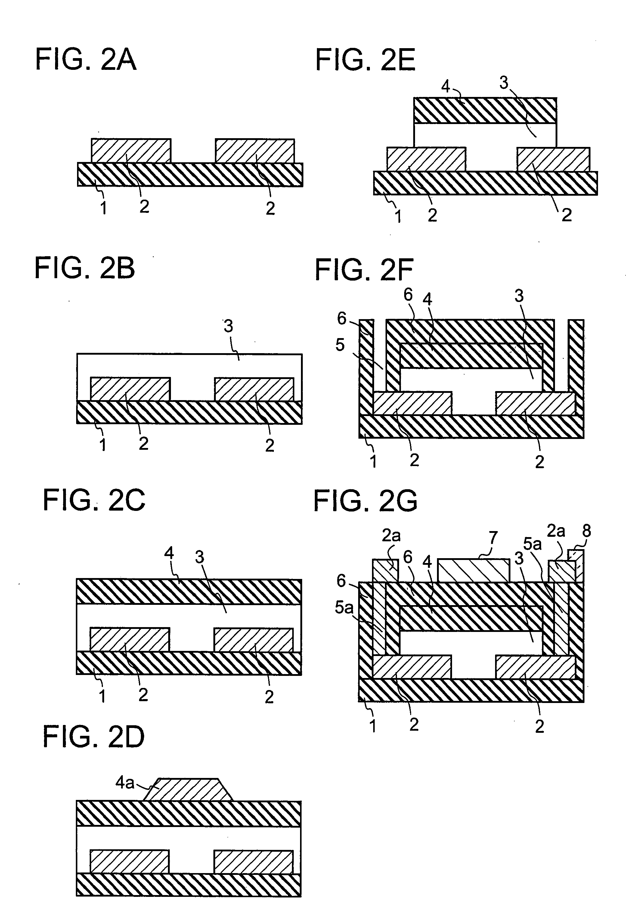
Semiconductor device including active layer made of zinc oxide with controlled orientations and manufacturing method thereof
a technology of zinc oxide and active layer, which is applied in the direction of semiconductor devices, basic electric elements, electrical apparatus, etc., can solve the problems of insufficient electron mobility, crystal distortion, crystal distortion, etc., and achieve the effects of improving heat resistance, microfabrication properties, and surface smoothness
- Summary
- Abstract
- Description
- Claims
- Application Information
AI Technical Summary
Benefits of technology
Problems solved by technology
Method used
Image

Examples
examples
[0059] Hereinafter, the experimental examples for evaluating the oxide semiconductor thin film layer of the semiconductor device according to the present invention will be shown, to clarify the effects of the present invention. The oxide semiconductor thin film layer used in the examples below was formed by means of magnetron sputtering while applying a constant 180 W of input electric power having a frequency of 13.56 MHz to the target and applying various bias electric powers having a frequency of 13.56 MHz to the substrate via a substrate stage.
[0060]FIG. 3 shows the X-ray diffraction intensity as a function of different bias electric powers applied to the substrate during zinc oxide film formation of the oxide semiconductor thin film layer. Specifically, the oxide semiconductor thin film layer was formed with different bias electric powers of 0 W, 1 W, 2 W, 5 W, 10 W, 20 W, 40 W, and 80 W. In other words, the oxide semiconductor thin film layer was formed without applying bias ...
PUM
 Abstract
Description
Claims
Application Information