CDMA power amplifier design for low and high power modes

a power amplifier and low power mode technology, applied in the direction of amplifier combinations, high frequency amplifiers, gain control, etc., can solve the problems of low power mode response, low power mode operation, etc., to improve the response in hp mode, improve the performance of the power amplifier, and reduce the loss of insertion

Inactive Publication Date: 2007-08-16
SKYWORKS SOLUTIONS INC
View PDF5 Cites 31 Cited by
  • Summary
  • Abstract
  • Description
  • Claims
  • Application Information

AI Technical Summary

Benefits of technology

[0026] The drawbacks and shortcomings described previously are overcome by the disclosed invention by providing a variable load circuit to provide a two-state or multi-state load design. For example, low impedance is provided for high power operation and a high impedance state provided for low power operation. The load is adjusted via a “switching” operation based, in part, on the operating power level of the amplifier. In order to achieve improved efficiency performance at lower output power levels, the output device needs to “see” a higher impedance load. This follows from the fact that higher load impedance reduces the current swing for the low power mode. On the other hand, providing low impedance at high power levels avoids sacrificing efficiency at higher power levels.
[0029] In another aspect, the invention includes embodiments with a switchable cubic predistortion linearizer (SCPDL) to improve the response in the higher power modes. A switch responsive to a signal for selecting a power mode also triggers the appropriate SCPDL functionality to improve the performance. Preferably, in two power mode designs, the lower power mode does not require SCPDL action and the transition to the high power mode also includes activation of the SCPDL. Preferably, SCPDL is placed at about the input of the power amplifier to better shape the input signal. Similar placement of a dual harmonic filter is also possible to reduce spurs and allow for other signal shaping, for instance, to correct signal distortions due to a transreceiver.
[0031] In one aspect, the amplifier load circuit may include a plurality of transmission line segments to provide suitable loads in different frequency bands with a harmonic filter or a dual resonance harmonic filter coupled between the load circuit input node and a common node; a first capacitor coupled between the first node and the common node; a first switch coupled between the common node and ground; and a second capacitor and a second switch connected to one another in series between the second node and ground; wherein the first switch is responsive to said power mode signal and the second switch is responsive to a band select signal to further improve amplifier efficiency in the low power mode(s).
[0032] In another aspect, while the use of one or two switches is described, additional switches may be used, preferably, to implement a plurality of power levels and frequency bands of operation. The number of switches is preferably kept low to reduce switching losses. In addition, a single switch may respond to both the power mode and band select signal or multiple switches may respond to a power mode or band select signal.
[0035] Alternatively, the harmonic filter may, preferably, be a dual harmonic filter, which exhibits higher impedance at the fundamental than the series LC filter and low impedance at the second harmonic. The high impedance at the fundamental exhibited by a dual resonance harmonic filter prevents detuning in the low power mode while leaving the load matching properties relatively unaffected.
[0042] In another aspect, an embodiment includes a switchable cubic predistortion linearizer (“SCPDL”) to further improve the response in the HP mode. Preferably, the SCPDL is responsive to a power mode select signal such that it contributes little more than a small insertion loss when the power amplifier is in a low power mode. However, when the power amplifier is in a high(er) power mode, SCPDL is invoked and improves the performance of the power amplifier. Preferably, SCPDL is coupled directly or indirectly to the input stage of the power amplifier. In combination with the choice of a suitable output impedance for the low power mode, an efficient and effective filter for removing one or more selected harmonics, SCPDL provides a power amplifier that provides an improved response in both the high power and low power modes.

Problems solved by technology

An undesirable side effect of providing this low impedance is that it often leads to a degraded efficiency when the output power level is low.
The power amplifiers in these devices, however, are optimized for the high power mode with the low power mode operations, when present, being relatively inefficient.
Such improvement at high power levels, however, also results in reduced average power efficiency due to reduced efficiency in the low power mode, which was noted to be the mode in which 95% of time was spent by CDMA sets.
Thus, the typical design of power amplifiers, although optimized for high power mode, actually results in reduced battery life.
The prior art does not teach or suggest selecting the output matching impedance to improve operation at an output power levels other than at high power even though CDMA phones actually spend an overwhelming amount of their operational time in relatively lower power modes.
The high power performance of a power amplifier is often compromised by the distortion or noise generated as a result of such an operation.
Using a predistortion linearizer adversely impacts the performance in lower power modes due to the weak input signals.
Such limitations on the use of predistortion linearizers require that a choice be made between superior performance in a high power mode and the performance in a lower power mode.

Method used


Image

  • CDMA power amplifier design for low and high power modes
  • CDMA power amplifier design for low and high power modes
  • CDMA power amplifier design for low and high power modes

Examples


Embodiment Construction

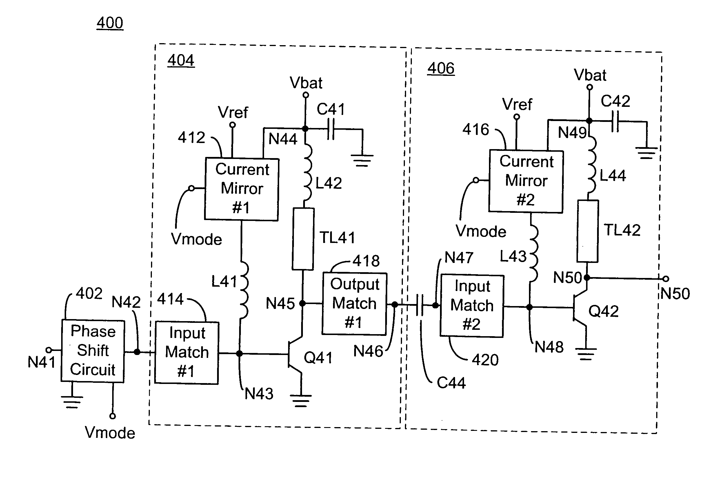
[0061]FIG. 4 shows power amplifier 400 in accordance with the present invention. Power amplifier 400 can serve as the power amplifier portion of power amplifier / load circuit 124 seen in FIG. 1. An RF signal input to power amplifier 400 at input node N41 may be phase shifted by phase shift circuit 402, first amplifier stage 404, and second amplifier stage 406, before exiting at output node N50.

[0062] Phase shift circuit 402 helps minimize phase discontinuity when switching between HP and LP modes in order to preserve phase coherency of the output signal. The RF signal at output node N42 is phase shifted relative to the signal at input node N41 depending on the Vmode signal.

[0063] As is known to those skilled in the art, the Vmode signal is a voltage level controlled by a dictated controller, such as a processor or the like, belonging to the device in which the power amplifier is resident. In the present invention such a controller (not shown) changes the value of the Vmode signal w...


PUM


Abstract

An amplifier circuit responsive to a power mode signal improves efficiency at low power levels without compromising efficiency at high power levels. At low power levels, high impedance is presented with suitable adjustment in the phase of the signal. Also, providing for predistortion linearization improves high power efficiency and switching the predistortion linearizer OFF at low power levels contributes little more than a small insertion loss. The power amplifier also uses a bias circuit incorporating a dual harmonic resonance filter to provide high impedance at a fundamental frequency and low impedance at a second harmonic. These properties are of particularly advantageous since amplifiers in cell-phones are used in low power modes most of the time although they are designed to be most efficient at primarily the highest power levels.

Description

BACKGROUND OF THE INVENTION [0001] 1. Field of the Invention [0002] The present invention relates generally to the field of power amplifiers in multi-band communication systems. More particularly, the present invention relates to circuitry associated with such power amplifiers, such as harmonic filters, impedance load switching circuits, pre-distortion phase filters, and the like. [0003] 2. Description of the Related Art [0004] Several digital air interface standards have been developed for providing efficient digital communication of voice, data, fax and text messages under the umbrella of “personal communications services” or PCS. Operational PCS systems, such as systems based on the GSM TDMA (Time Division Multiple Access) or IS-95 CDMA (Code Division Multiplex Access) air interface standards, are being implemented in the United States in the 1900 MHz frequency range. Meanwhile, existing analog (AMPS) and digital (D-AMPS) at 800 MHz cellular systems continue to operate. Thus, the...

Claims


Application Information

Patent Timeline
Patent Type & Authority Applications(United States)
IPC IPC(8): H03G3/20H03F1/14H03F3/191H03F3/60
CPCH03F1/14H03F1/30H03F1/3241H03F1/56H03F2200/75H03F3/191H03F3/60H03F2200/318H03F2200/411H03F3/189
Inventor DOW, GEE SAMUELBAO, JIANWENHUANG, CHUN-WEN PAUL
Owner SKYWORKS SOLUTIONS INC
Why Eureka
Try Eureka