Manufacturing method of semiconductor device

Inactive Publication Date: 2007-08-16
KK TOSHIBA
View PDF5 Cites 12 Cited by
  • Summary
  • Abstract
  • Description
  • Claims
  • Application Information

AI Technical Summary

Problems solved by technology

However, when the thickness of a silicon oxide film or silicon nitride film that has conventionally been used is reduced, a leakage current is increased, thus restricting the film thickness reduction.
However, the decomposition efficiencies of the above silicon sources are low, so that nitrogen or carbon contained in the silicon source may be introduced into the silicate film as impurity.
This may result in an increase of the leakage current or occurrence of a fixed charge, causing degradation of the characteristics and reliability of a semiconductor device.
However, the de

Method used


Image

  • Manufacturing method of semiconductor device
  • Manufacturing method of semiconductor device
  • Manufacturing method of semiconductor device

Examples


first embodiment

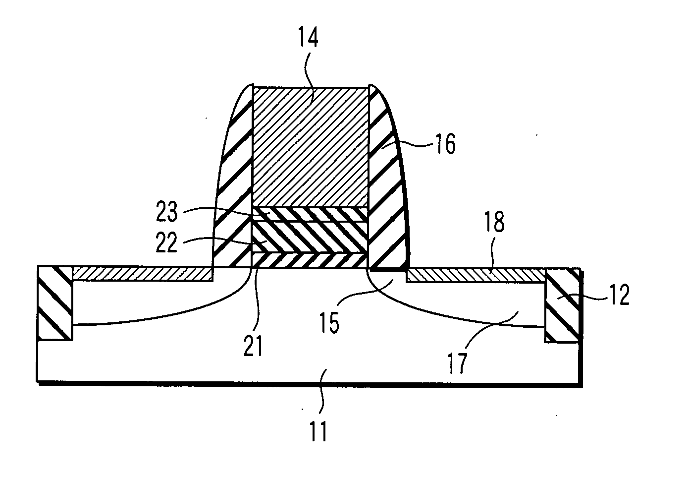
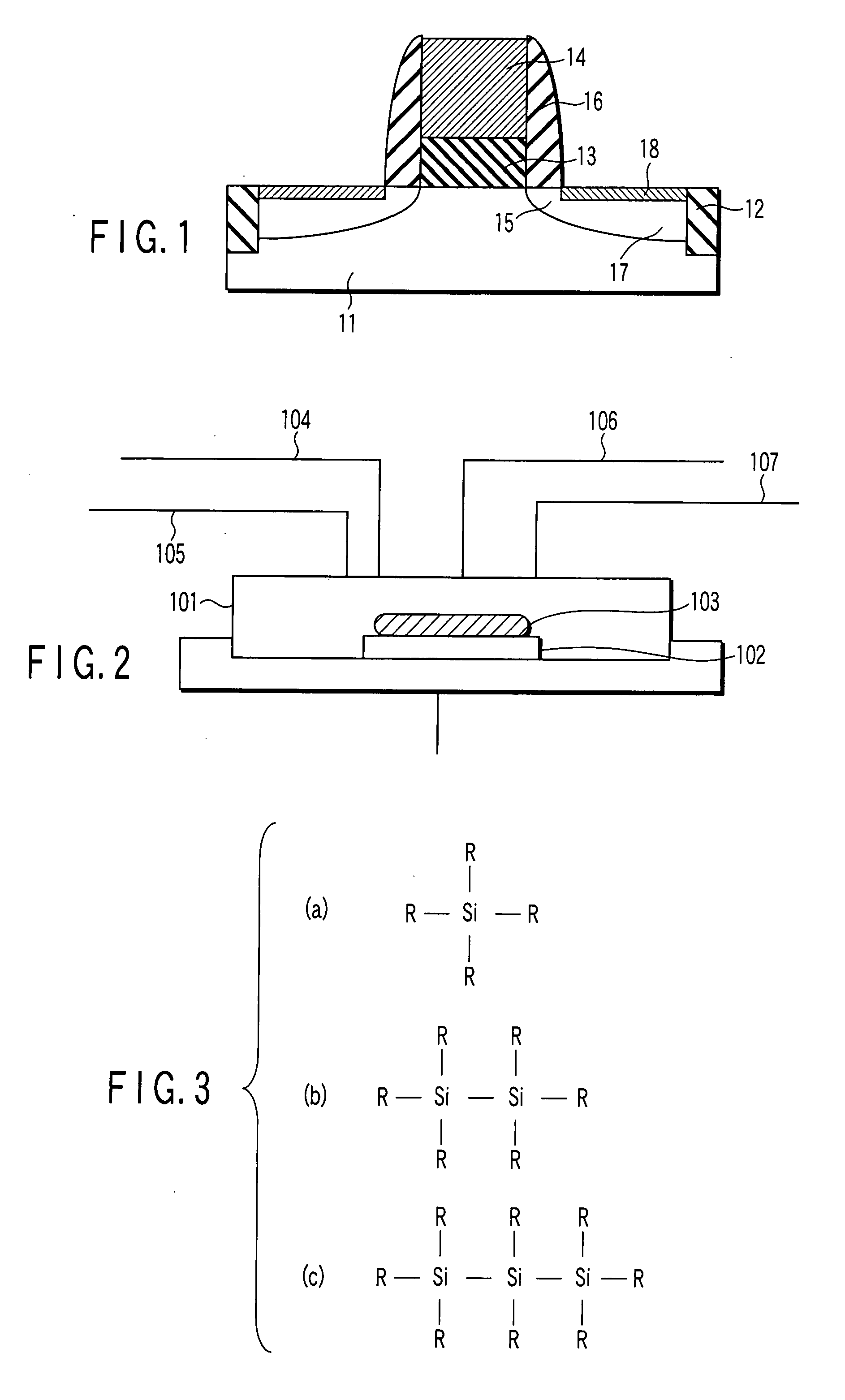
[0024]FIG. 1 is a cross-sectional view schematically showing a structure of a semiconductor device (MIS transistor) according to a first embodiment of the present invention.

[0025] A manufacturing method of the semiconductor device shown in FIG. 1 will briefly be described below. An isolation region 12 is formed in the surface region of a silicon substrate (semiconductor substrate) 11. Subsequently, a gate insulating film 13 is formed on the silicon substrate 11 and a gate electrode 14 is formed on the gate insulating film 13. Subsequently, after a shallow impurity diffusion layer 15 which becomes a source / drain region is formed, a side wall insulating portion 16 is formed on the side surface of the gate insulating film 13 and gate electrode 14. Further, after a deep impurity diffusion layer 17 which becomes a source / drain region is formed, a silicide film (salicide film) 18 is formed on the surface of the source / drain region. In this manner, the semiconductor device shown in FIG. 1...

second embodiment

[0056] A semiconductor device (MIS transistor) according to a second embodiment of the present invention will be described.

[0057] The basic structure of the semiconductor device according to the second embodiment and basic manufacturing method thereof are the same as those of the semiconductor device according to the first embodiment shown in FIG. 1, and the detailed descriptions thereof are omitted here.

[0058] The details of the formation method of a gate electrode 14 (refer to FIG. 1) will next be described.

[0059] In the present embodiment, the gate electrode 14 is formed of a metal silicide film. Silicon and a metal element are contained in the metal silicide film. In addition to silicon and metal element, Nitrogen (N) may be contained in the metal silicide film. Specifically, a hafnium (Hf) silicide film, a zirconium (Zr) silicide film, a tantalum (Ta) silicide film, a titanium (Ti) silicide film, a ruthenium (Ru) silicide film, or a tungsten (W) silicide film can be used as ...


PUM


Abstract

A method of manufacturing a semiconductor device, includes forming a gate insulating film on a semiconductor substrate, and forming a gate electrode on the gate insulting film, wherein forming the gate insulating film includes forming a metal silicate film, and a silicon source used for forming the metal silicate film includes at least one of a first hydrocarbon silicon compound obtained by replacing at least one of hydrogen atoms in monosilane with an alkyl group, a second hydrocarbon silicon compound obtained by replacing at least one of hydrogen atoms in disilane with an alkyl group, and a third hydrocarbon silicon compound obtained by replacing at least one of hydrogen atoms in trisilane with an alkyl group.

Description

CROSS-REFERENCE TO RELATED APPLICATIONS [0001] This application is based upon and claims the benefit of priority from prior Japanese Patent Applications No. 2006-023838, filed Jan. 31, 2006; and No. 2006-322101, filed Nov. 29, 2006, the entire contents of both of which are incorporated herein by reference. BACKGROUND OF THE INVENTION [0002] 1. Field of the Invention [0003] The present invention relates to a manufacturing method of a semiconductor device. [0004] 2. Description of the Related Art [0005] Along with miniaturization of a semiconductor device, there is an increasing demand for a reduction in thickness of a gate insulating film. However, when the thickness of a silicon oxide film or silicon nitride film that has conventionally been used is reduced, a leakage current is increased, thus restricting the film thickness reduction. [0006] In light of the above, there is proposed that a metal silicate film (e.g., Hf-silicate film) having a relative dielectric constant higher than...

Claims


Application Information

Patent Timeline
IPC IPC(8): H01L21/4763
CPCH01L21/28194H01L29/517H01L29/513H01L29/4975
Inventor SATO, MOTOYUKIAOYAMA, TOMONORI
Owner KK TOSHIBA
Why Eureka
Try Eureka