Low resistance tunnel junctions in wide band gap materials and method of making same

Active Publication Date: 2007-08-23
CREE INC
View PDF4 Cites 28 Cited by
  • Summary
  • Abstract
  • Description
  • Claims
  • Application Information

AI Technical Summary

Benefits of technology

[0026]FIG. 6 is a band gap diagram illustrating the energy bands of a device similar to that seen i

Problems solved by technology

Unfortunately, there is an upper limit to how much this mechanism can reduce the tunnel width.
All dopants eventually reach a saturation solubility limit at which the material is no longer capable of absorbing further dopants without changing its composition.
Once this saturation limit is reached, doping loses its ability to reduce the tunnel width.
Furthermore, as the charge density increases the dopant ionizat

Method used


Image

  • Low resistance tunnel junctions in wide band gap materials and method of making same
  • Low resistance tunnel junctions in wide band gap materials and method of making same
  • Low resistance tunnel junctions in wide band gap materials and method of making same

Examples


Embodiment Construction

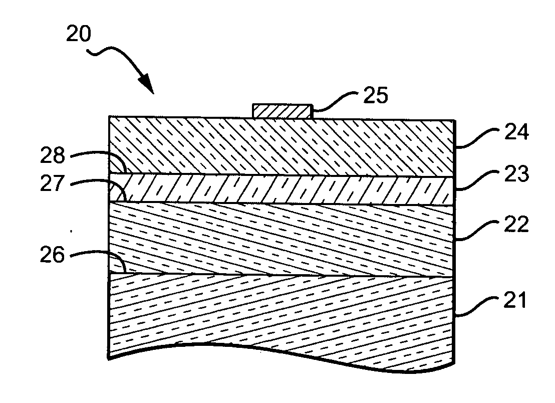
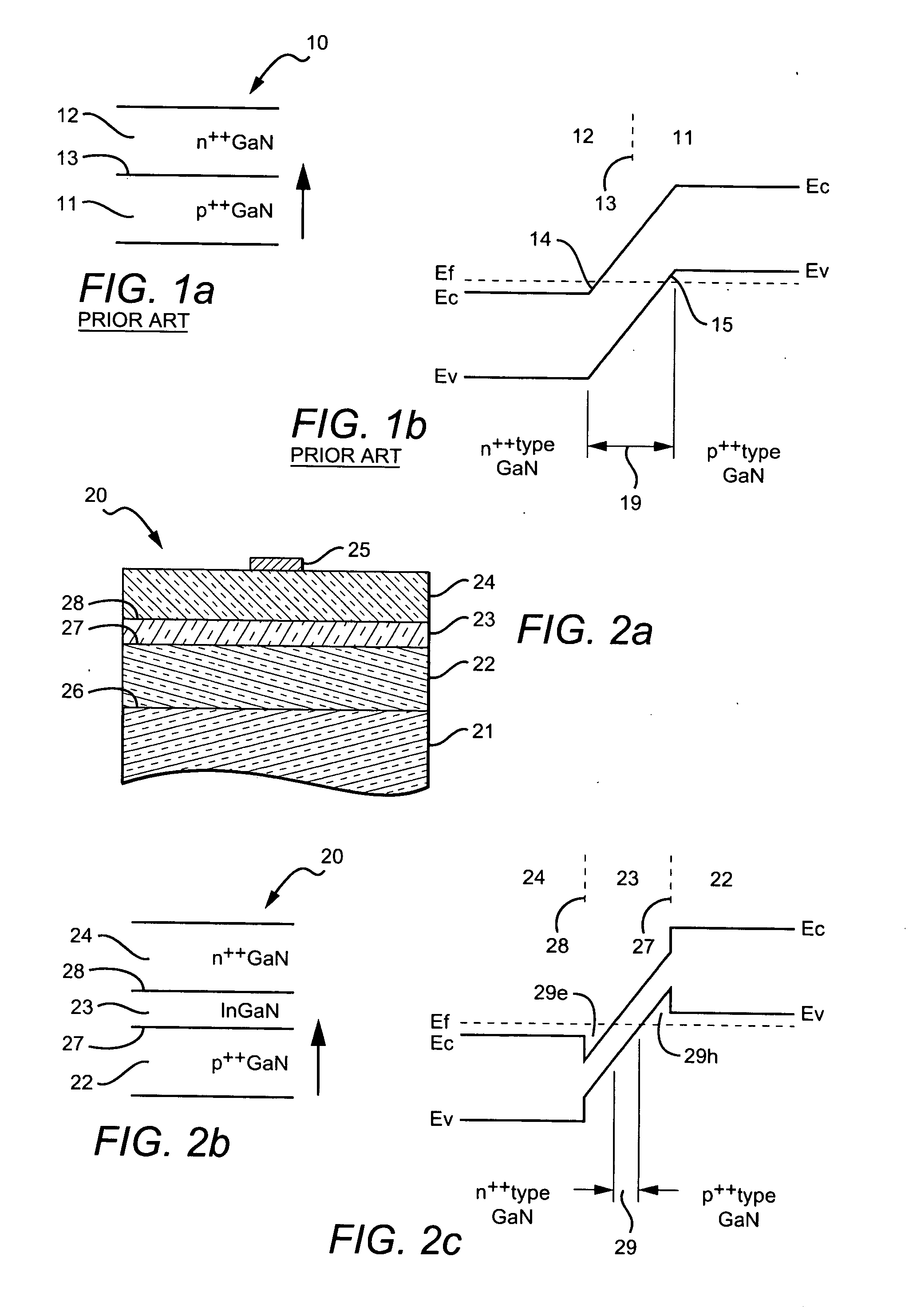
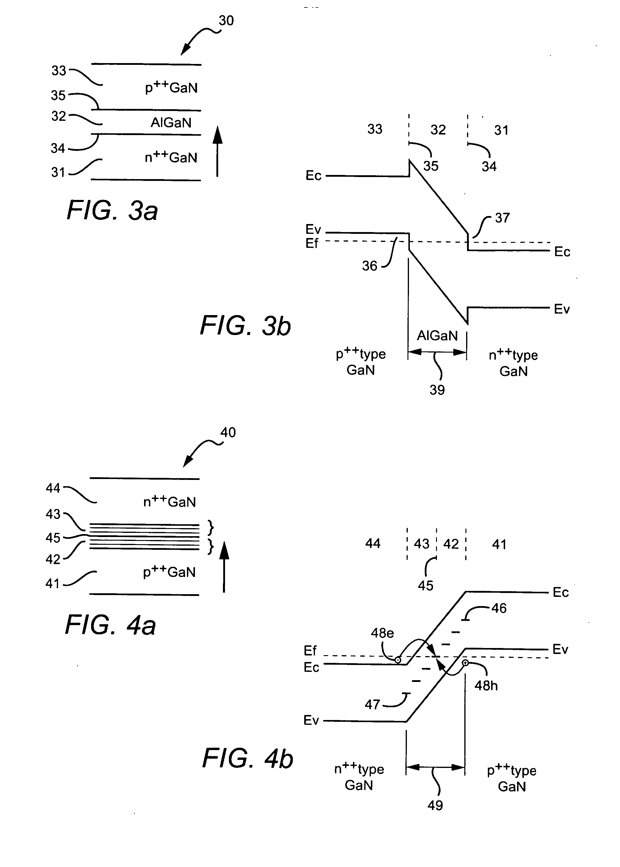
[0027] The present invention is a low resistance tunnel junction structure in wide band gap materials. It will be understood, however, that the structures disclosed apply to semiconductor tunnel junction structures in general, where low resistance is desired, but in the absence of the present technique unavailable. These junctions may be fabricated from periodic table of the elements groups III-V and II-VI compound semiconductors, whose crystal layers are grown normal to a polar direction of the crystal. In one embodiment, the tunnel junction structures are presumed to have the Wurtzite crystal structure with layers comprising gallium nitride GaN, indium gallium nitride InxGayN, and aluminum gallium nitride AlxGayN where 0.3≦x≦1.0 and x+y=1.0. In this embodiment, except where noted, the top surface of the crystal has (0001) orientation with Periodic Table group III polarity.

[0028] In preferred embodiments, all of the layers are prepared by epitaxial growth methods, although it will...


PUM


Abstract

A low resistance tunnel junction that uses a natural polarization dipole associated with dissimilar materials to align a conduction band to a valence band is disclosed. Aligning the conduction band to the valence band of the junction encourages tunneling across the junction. The tunneling is encouraged, because the dipole space charge bends the energy bands, and shortens a tunnel junction width charge carriers must traverse to tunnel across the junction. Placing impurities within or near the tunnel junction that may form deep states in the junction may also encourage tunneling in a tunnel junction. These states shorten the distance charge carriers must traverse across the tunnel junction.

Description

BACKGROUND OF THE INVENTION [0001] 1. Field of the Invention [0002] The present invention relates to semiconductor devices formed in wide band gap materials, and in particular to fabricating low resistance tunnel junctions in wide band gap materials. [0003] 2. Description of the Related Art [0004] Junctions between differently doped regions of a single semiconductor material are called homojunctions. These junctions are formed, for example, when a single material abruptly transitions from one type of doping to another. An abrupt transition is typically one where a value of merit (in this instance doping concentration) changes by more than one percent per monolayer. [0005] A p-n homojunction consists of a p-type and an n-type section of the same semiconductor materials in metallurgical contact with each other. When n- and p-type semiconductors are brought into contact to form a junction, electrons and holes diffuse from areas of high concentration towards areas of low concentration. ...

Claims


Application Information

Patent Timeline
IPC IPC(8): H01L29/08
CPCH01L29/2003H01L29/88H01L29/205
Inventor IBBETSON, JAMES P.KELLER, BERND P.MISHRA, UMESH K.
Owner CREE INC
Why Eureka
Try Eureka