Bremsstrahlung laser ("blaser")

a laser and beam beam technology, applied in the field of lasers, can solve the problems of large, complex apparatus, and high cost of laser radiation generators, and achieve the effect of improving the probability of electron tunneling

Inactive Publication Date: 2008-01-10
CALIFORNIA INST OF TECH
View PDF3 Cites 28 Cited by
  • Summary
  • Abstract
  • Description
  • Claims
  • Application Information

AI Technical Summary

Benefits of technology

[0010] In one embodiment, the region between the at least two waveguide elements comprises a region devoid of matter to provide a vacuum condition therein. In one embodiment, the region between the at least two waveguide elements is filled with an insulating material. In one embodiment, the insulating material is a nanostructured material. The nanostructured material, such as a quantum dot composite in polymer matrix, can be designed to enhance the tunneling probability of the electrons moving between the two sides of the waveguides. In one embodiment, the Bremsstrahlung radiation is light. In one embodiment, the light is coupled to an optical mode of the at least two waveguide elements. In one embodiment, the provided apparatus further comprises an optical source. In one embodiment, the provided apparatus further comprises an optical amplifier. In one embodiment, the provided apparatus further comprises optical feedback. In one embodiment, the Bremsstrahlung radiation is laser radiation. In one embodiment, the radiation is X-ray or UV radiation. In one embodiment, the radiation is infrared or terahertz radiation.

Problems solved by technology

As will be immediately recognized upon reviewing the literature on free electron lasers, the apparatus needed to generate such laser radiation is complex, large, and expensive.

Method used


Image

  • Bremsstrahlung laser ("blaser")
  • Bremsstrahlung laser ("blaser")
  • Bremsstrahlung laser ("blaser")

Examples


example 1

High-Q Ring Resonators in Thin Silicon-on-Insulator

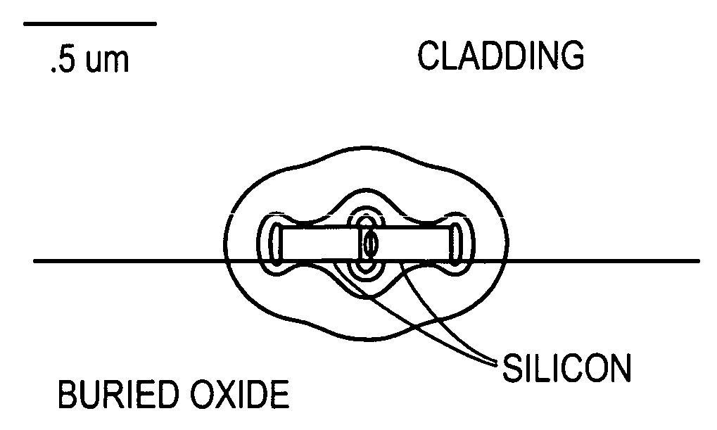
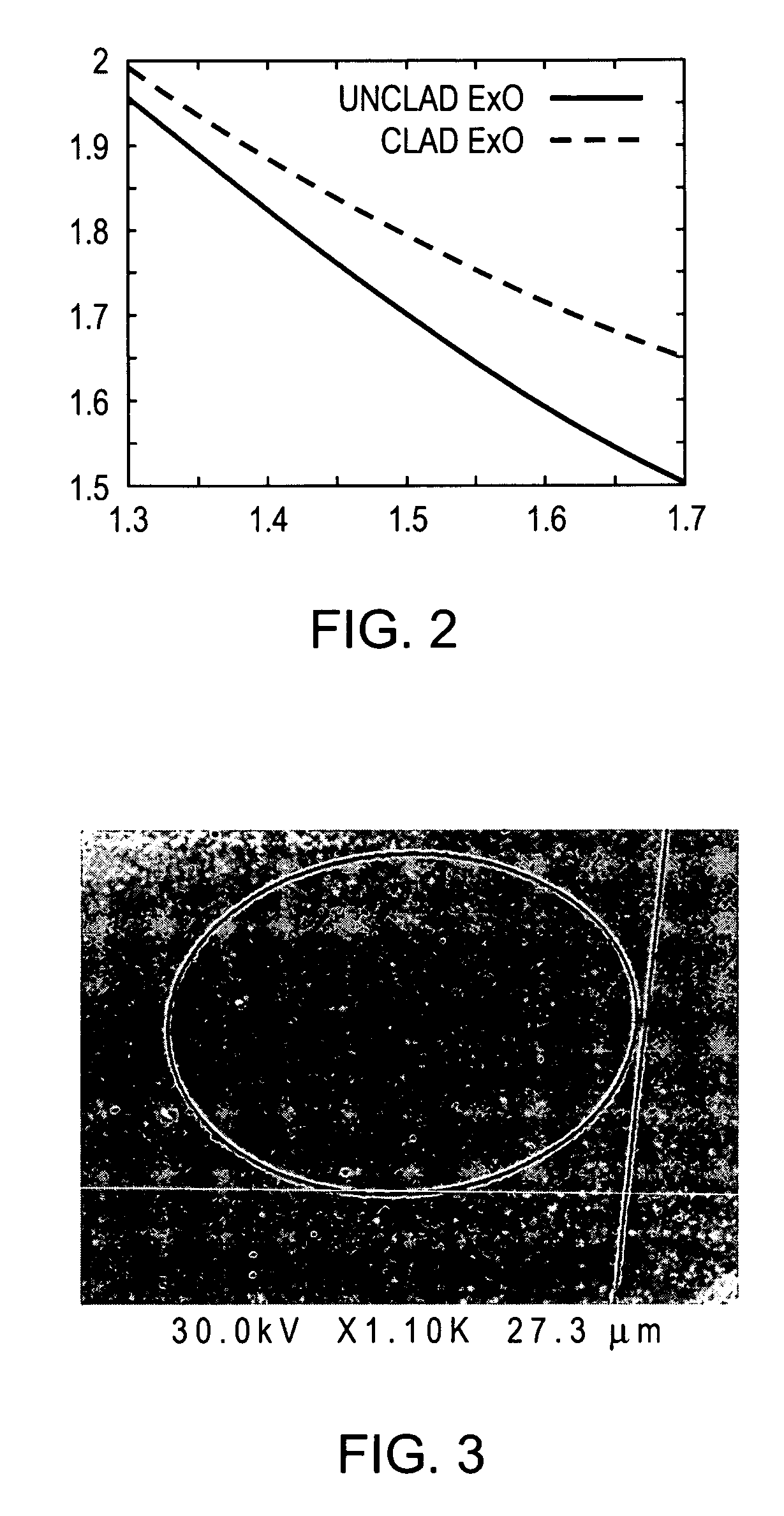
[0058] Resonators comprising high-Q microrings were fabricated from thin silicon-on-insulator (SOI) layers. Measured Q values of 45 000 were observed in these rings, which were then improved to 57 000 by adding a PMMA cladding. Various waveguide designs were calculated, and the waveguide losses were analyzed.

[0059] Microring resonator structures as laser sources and as optical filter elements for dense wavelength division multiplexing systems have been studied in the past. The silicon-on-insulator (SOI) structure described here is particularly advantageous. It has low waveguide loss. One can extrapolate an uncoupled Q value of 94 000 and a waveguide loss of 7.1 dB / cm in the unclad case, and −6.6 dB / cm in the PMMA clad case, from the respective measured Q values of 45 000 and 57 000. Although higher Q values have been obtained for optical microcavities, we believe that our geometry has the highest Q for a resonator based on a singl...

example 2

High-Q Optical Resonators in Silicon-on-Insulator Based Slot Waveguides

[0067] We now describe the design, fabrication and characterization of high Q oval resonators based on slot waveguide geometries in thin silicon on insulator material. Optical quality factors of up to 27,000 were measured in such filters, and we estimate losses of −10 dB / cm in the slotted waveguides on the basis of our resonator measurements. Such waveguides enable the concentration of light to very high optical fields within nano-scale dimensions, and show promise for the confinement of light in low-index material with potential applications for optical modulation, nonlinear optics and optical sensing. As will be appreciated, the precise geometry of a resonator (or other kinds of devices) is frequently a matter of design, and the geometry can be varied based on such considerations as length of waveguide, area of a chip, and required interaction (or required non-interaction), such as coupling (or avoiding coupli...

examples 1-4

Four-Wave Mixing in Silicon Waveguides with χ3 Polymer Material

[0083] Two types of integrated nano-optical silicon waveguide structures were used for this demonstration. The first type of structure was a series of ring resonator structures, which allowed an estimation of the waveguide loss of the nonlinear material. The second type of structures used were long runout devices, which comprised a simple waveguide loop with distances on the order of 0.7 cm. Characterization of loss could be done passively.

[0084] For the actual nonlinear testing, a Keopsys EDFA was used to boost two lasers to a high power level, on the order of 30 dBm (1 Watt) or more.

[0085] The materials used for the demonstrations were clad on waveguides configured as previously described herein. The chromophore identified as JSC1 is shown by its chemical structure in FIG. 27. The chromophores identified as JSC1 and YLD 124 are two substances among many chromophores that were described in a paper by Alex Jen, et al....


PUM


Abstract

A light generating system that comprises a narrow evacuated slot defined between at least two high index contrast waveguide elements. The apparatus can be fabricated using a material such as a SOI wafer having an oxide layer thickness of the order of 1 micron and a top silicon layer thickness of the order of 100-150 nm. Electrode contacts are provided to at least two waveguide elements fabricated in the top silicon layer, each waveguide element having a thickness comparable to the top silicon layer thickness, a width of some hundreds of nm, and having a slot having dimensions in the range of 50-200 nm defined therebetween. The length of the slot is at least as long as the slot width. Charged particles, such as electrons, that are emitted and accelerated across the slot by an applied electrical signal provide a source of photons as a consequence of being accelerated and/or decelerated.

Description

CROSS-REFERENCE TO RELATED APPLICATIONS [0001] This application claims priority to and the benefit of co-pending U.S. provisional patent application Ser. No. 60 / 694,569, filed Jun. 28, 2005 which application is incorporated herein by reference in its entirety.STATEMENT REGARDING FEDERALLY FUNDED RESEARCH OR DEVELOPMENT [0002] The invention described herein was made in the performance of work under Air Force Office of Scientific Research Grant F49620-03-1-0418, and is subject to the provisions of Public Law 96-517 (35 U.S.C. §202) in which the Contractor has elected to retain title.FIELD OF THE INVENTION [0003] The invention relates to lasers in general and particularly to a laser that employs charged particles undergoing acceleration as a source of electromagnetic radiation. BACKGROUND OF THE INVENTION [0004] Electron lasers have been described in the literature for some time. In particular, John M. J. Madey (B. S. Physics Caltech 1964, M. S. Electrical Engineering Caltech 1965) is ...

Claims


Application Information

Patent Timeline
Patent Type & Authority Applications(United States)
IPC IPC(8): H01S3/00
CPCH01S3/063H01S3/0903H01S3/083
Inventor HOCHBERG, MICHAEL J.BAEHR-JONES, TOM
Owner CALIFORNIA INST OF TECH
Why Eureka
Try Eureka