Magnetic Tunnel Junction Device and Method of Manufacturing the Same

a tunnel junction and magnetic tunnel technology, applied in the field of magnetic tunnel junction devices, can solve the problems of signal loss in noise, inability to read signals, and too small output voltage when operating margins are considered for devices to be employed for actual memory devices, etc., and achieve the effect of enhancing the tunneling probabilities of carriers

Inactive Publication Date: 2007-11-08
JAPAN SCI & TECH CORP +1
View PDF10 Cites 32 Cited by
  • Summary
  • Abstract
  • Description
  • Claims
  • Application Information

AI Technical Summary

Benefits of technology

[0027] wherein the tunnel barrier layer is formed of a single-crystalline MgOx (001) or a poly-crystalline MgOx (0<x<1) layer in which the (001) crystal plane is preferentially oriented (to be hereafter referred to as “a MgO layer”), wherein the wave functions of conduction electrons in the first and / or the second ferromagnetic layer are caused to seep into the Δ1 band of the MgO layer such that the tunneling probabilities of the carriers are enhanced.

Problems solved by technology

With such characteristics, the output voltage when operation margins are taken into consideration is too small for the device to be employed for an actual memory device.
This has resulted in the problem that as the level of integration increases, signals are increasingly lost in noise and cannot be read.

Method used


Image

  • Magnetic Tunnel Junction Device and Method of Manufacturing the Same
  • Magnetic Tunnel Junction Device and Method of Manufacturing the Same
  • Magnetic Tunnel Junction Device and Method of Manufacturing the Same

Examples


first embodiment

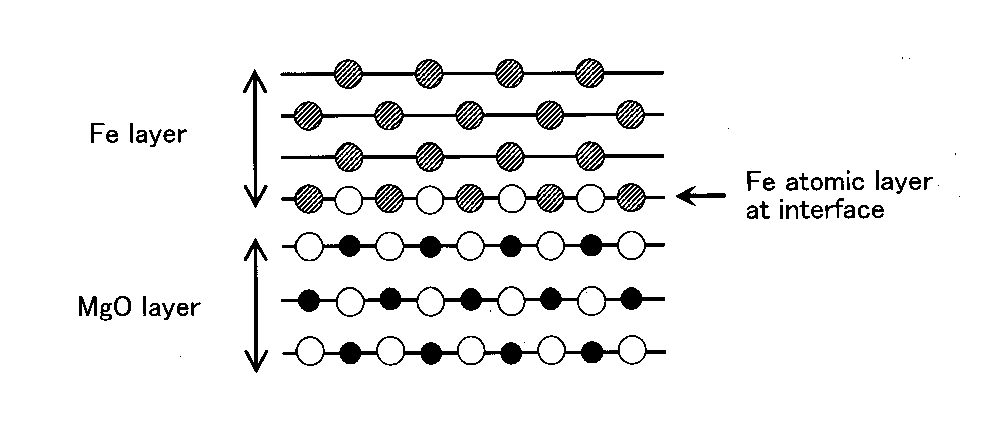
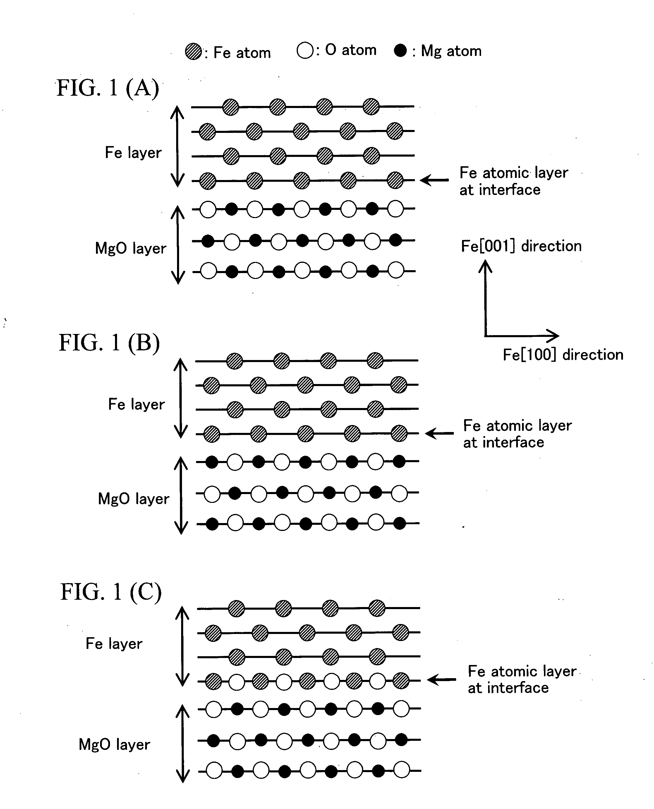
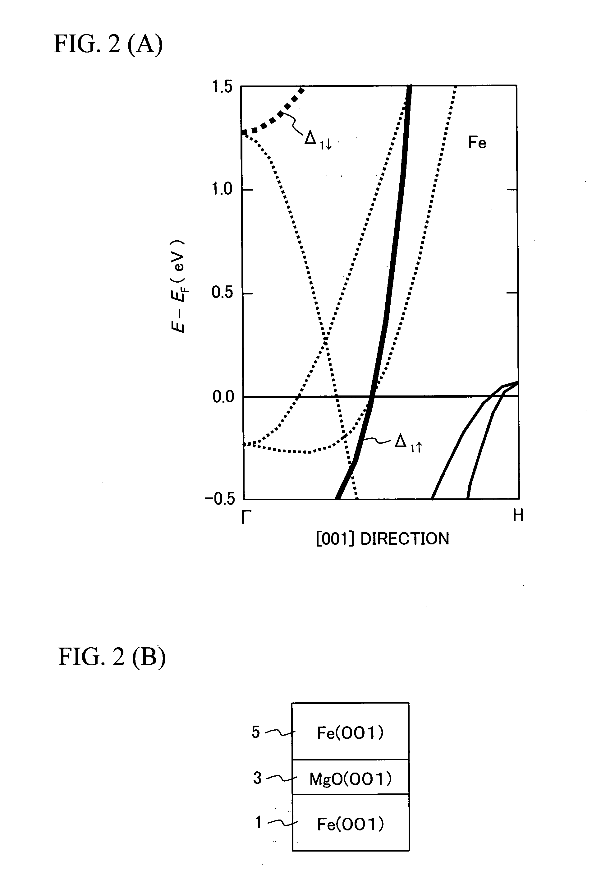
[0059] In the following, a MTJ device according to the invention and a method of manufacturing the same will be described with reference to the drawings. FIGS. 3(A) to 3(D) schematically show the method of manufacturing the MTJ device having the Fe (001) / MgO (001) / Fe(001) structure according to the embodiment (to be hereafter referred to as a “Fe(001) / MgO (001) / Fe(001) MTJ device”). Fe refers to a ferromagnetic material with the BCC structure. First, a single-crystalline MgO (001) substrate 11 is prepared. In order to improve the morphology of the surface of the single-crystalline MgO (001) substrate 11, a MgO (001) seed layer 15 is grown by the molecular beam epitaxy (MBE) method, for example. This is subsequently followed by the growth of an epitaxial Fe(001) lower electrode (first electrode) 17 with a thickness of 100 nm on the MgO (001) seed layer 15 at room temperature, as shown in FIG. 1(B). Annealing is then performed at 350° C. under ultrahigh vacuum (2×10⁻⁸ Pa), whereby the...

second embodiment

[0086] Hereafter, a magnetic tunnel junction device according to the invention and a method of manufacturing the same will be described. In the method of manufacturing a MTJ device according to the present embodiment, MgO (001) is initially deposited in a poly-crystalline or amorphous state by sputtering or the like, and then an annealing process is performed such that a polycrystal in which the (001) crystal plane is oriented or a single crystal is obtained. The sputtering conditions were such that, for example, the temperature was room temperature (293K), a 2-inch φ MgO was used as a target, and sputtering was conducted in an Ar atmosphere. The acceleration power was 200 W and the growth rate was 0.008 nm / s. Because MgO deposited under these conditions is in an amorphous state, a crystallized MgO can be obtained by increasing the annealing temperature to 300° C. from room temperature and maintaining that temperature for a certain duration of time.

[0087] An oxygen deficiency may be...


PUM

PropertyMeasurementUnit
thicknessaaaaaaaaaa
thicknessaaaaaaaaaa
thicknessaaaaaaaaaa

Abstract

A single-crystalline MgO (001) substrate 11 is prepared, and then an epitaxial Fe (001) lower electrode (first electrode) 17 with a thickness of 50 nm is grown on a MgO (001) seed layer 15 at room temperature. Annealing is then performed in ultrahigh vacuum (2×10⁻⁸ Pa) at 350° C. A 2-nm thick MgO (001) barrier layer 21 is epitaxially grown on the Fe (001) lower electrode (first electrode) 17 at room temperature, using electron beam evaporation of MgO. A Fe (001) upper electrode (second electrode) 23 with a thickness of 10 nm is then grown on the MgO (001) barrier layer 21 at room temperature, successively followed by the deposition of a IrMn layer 25 with a thickness of 10 nm on the Fe (001) upper electrode (second electrode) 23. The IrMn layer 25 is used for realizing an antiparallel magnetization alignment by giving an exchange-biasing field to the upper electrode 23. Thereafter, the above-prepared sample is subjected to microfabrication so as to obtain a Fe (001)/MgO (001)/Fe (001) MTJ device with an enhanced MR ratio.

Description

BACKGROUND OF THE INVENTION [0001] 1. Field of the Invention [0002] The present invention relates to a magnetic tunnel junction device and a method of manufacturing the same, particularly to a magnetic tunnel junction device with a high magnetoresistance and a method of manufacturing the same. [0003] 2. Description of Related Art [0004] Magnetoresistive random access memories (MRAMs) refer to a large-scale integrated memory circuit that is expected to replace the currently widely used DRAM memories. Research and development of MRAM devices, which are fast and non-volatile memory devices, are being extensively carried out, and sample products of a 4 Mbit MRAM have actually been delivered. [0005]FIG. 15 shows the structure and operation principle of a magnetic tunnel junction device (to be hereafter referred to as a “MTJ device”), which is the most important part of the MRAM. As shown in FIG. 15(A), a MTJ device comprises a tunneling junction structure in which a tunnel barrier (to be...

Claims


Application Information

Patent Timeline
Patent Type & Authority Applications(United States)
IPC IPC(8): G11B5/39
CPCH01L27/228H01L43/12H01L43/08H10B61/22H10N50/10H10N50/01H01L27/105
Inventor YUASA, SHINJI
Owner JAPAN SCI & TECH CORP
Why Eureka
Try Eureka