Palladium plating solution

a technology of palladium plating and solution, which is applied in the direction of liquid/solution decomposition chemical coating, coating, printed circuit manufacturing, etc., can solve the problems of more and more severe characteristics of this junction, and achieve excellent solder wettability, improve the barrier function of the palladium plating film, and improve the heat resistance of the junction

Active Publication Date: 2007-09-06
EEJA LTD
View PDF2 Cites 3 Cited by
  • Summary
  • Abstract
  • Description
  • Claims
  • Application Information

AI Technical Summary

Benefits of technology

[0009]However, with the trend toward the miniaturization of packages and high-density packaging designs, the thin-film designs and small-area designs of the junction itself are proceeding and, therefore, a junction capable of realizing a good junction condition even when the junction is subjected to a high-temperature thermal history is required. In particular, in performing junction by soldering, under the present circumstances, there is required, also from the standpoint of manufacturing efficiency, a technique capable of forming a junction having excellent heat resistance which enables good junction to be performed even when the junction is subjected to a high-temperature thermal history.
[0010]The present invention has been made against the above-described circumstances, and in a junction which has hitherto been adopted in packages and the like, i.e., a junction having the construction of a nickel plating film, a palladium plating film and a gold plating film on a surface of a conductor formed from a metal such as copper, the invention provides a plating solution capable of forming a palladium plating film which can further improve the junction characteristics of the junction. In particular, in performing junction by soldering, the invention provides a plating solution capable of forming a palladium plating film which becomes a junction having excellent heat resistance.
[0011]To solve the above-described problems, the present inventors devoted themselves to repeated researches on a palladium plating solution capable of forming a palladium plating film. As a result, they found out that by adding germanium to a palladium plating solution containing a soluble palladium salt and an electrically conductive salt, the barrier action of the palladium plating film is improved, and have reached the present invention.

Problems solved by technology

However, as a result of the recent progress in miniaturization and high-density packaging techniques for electronic parts and semiconductor parts, characteristics required of this junction have become more and more severe than ever.

Method used


Image

  • Palladium plating solution
  • Palladium plating solution

Examples


Embodiment Construction

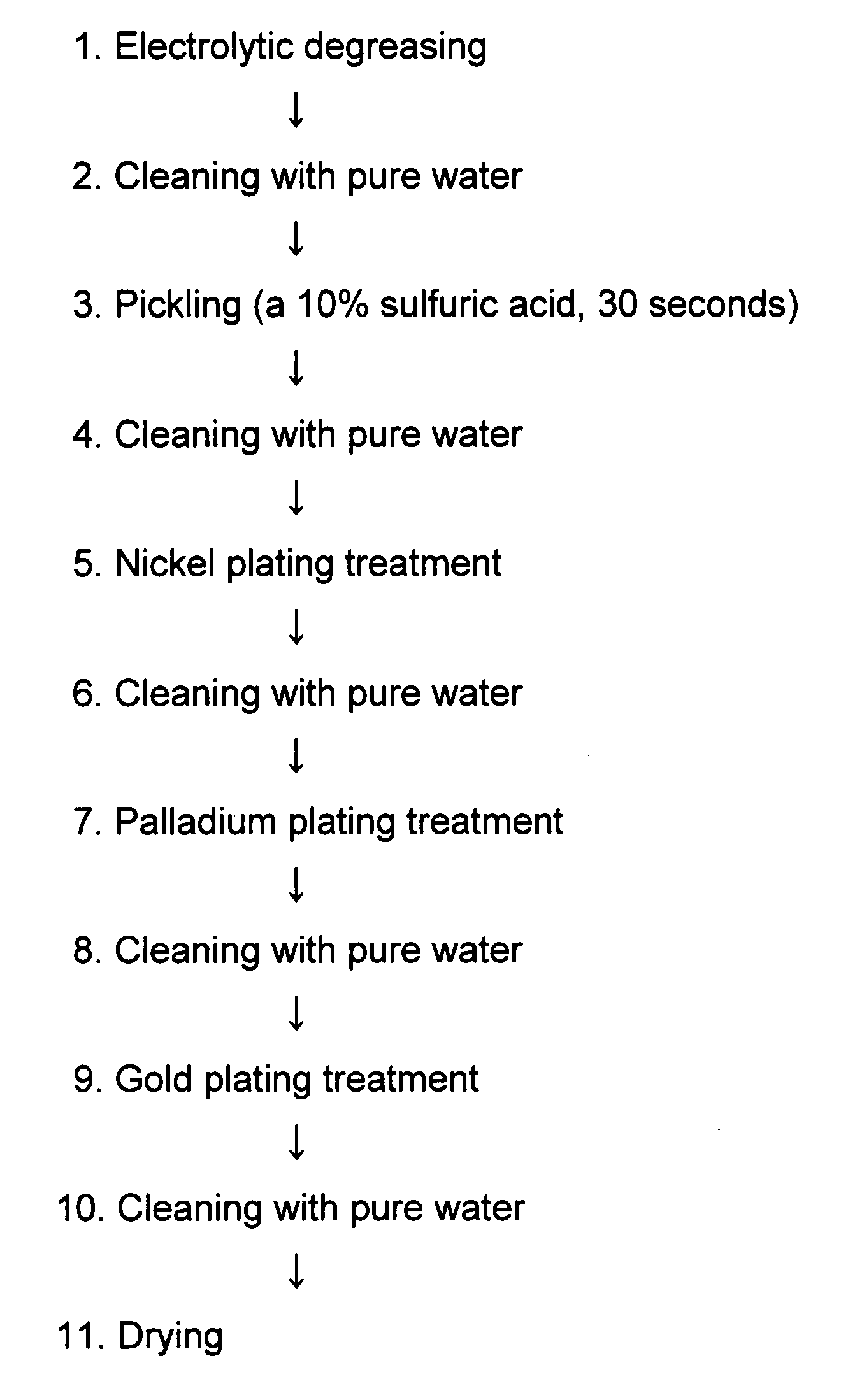
[0024]Preferred embodiments of the present invention will be described below on the basis of actual examples carried out.

[0025]In the embodiments, a junction to a solder is formed by using a palladium plating solution of the present invention, the evaluation of solder wettability is performed, and a description will be given of results of an investigation into the effectiveness of a palladium plating film.

[0026]In the evaluation of solder wettability, a Cu alloy-based lead frame on the surface of which a junction was formed by the plating treatment of a nickel plating film, a palladium plating film and a gold plating film in order was used as an evaluation sample. Each of the plating treatment conditions used in forming this junction is described below.

(Target film thickness: 0.7 μm)SULARMEX 100 (made by Electroplating Engineers of Japan Ltd., liquidcomposition: a plating solution containing nickel sulfamate)Liquid temperature55° C.Current density3 A / dm2 (Target film thickness: 0.0...


PUM

PropertyMeasurementUnit
current densityaaaaaaaaaa
pHaaaaaaaaaa
temperatureaaaaaaaaaa

Abstract

The invention provides a plating solution capable of forming a palladium plating film which can further improve solder characteristics in surface treatment of a composition made of a nickel plating film, a palladium plating film and a gold plating film on a surface of a conductor formed from a metal such as copper. In a palladium plating solution of the invention containing a soluble palladium salt and an electrically conductive salt having a liquid composition containing germanium, the amount of the soluble palladium salt is 0.1 g / l to 50 g / l in terms of a reduced value of palladium metal, the amount of the electrically conductive salt is 10 g / l to 400 g / l and the amount of the germanium is 0.1 mg / l to 1000 mg / l.

Description

BACKGROUND OF THE INVENTION[0001]1. Field of the Invention[0002]The present invention relates to a palladium plating solution and, more particularly, to a palladium plating film which provides a junction with a junction material, such as a solder.[0003]2. Description of the Related Art[0004]In recent years, as electronic parts and semiconductor parts there have been various things such as a printed circuit board and a package. Examples of what are called packages include a lead frame, a BGA (ball grid array), an LGA (land grid array package), a QFP (quad flat package), a minimold package and the like. To meet requirements for high-density packaging, these packages have been improved day by day to adapt to miniaturization and multi-pin designs and characteristics required of them tend to be increasingly severe.[0005]In such electronic parts and semiconductor parts, solders and bonding wires have hitherto been used as their junction materials, and soldering and wire bonding have been ...

Claims


Application Information

Patent Timeline
Patent Type & Authority Applications(United States)
IPC IPC(8): C25D3/50
CPCC25D3/50H05K3/244C25D5/12C25D3/567
Inventor WATANABE, SHINGOOHNISHI, JUNJIWACHI, HIROSHISONE, TAKAYUKI
Owner EEJA LTD
Why Eureka
Try Eureka