Electronic fuse with conformal fuse element formed over a freestanding dielectric spacer

Inactive Publication Date: 2007-09-13
IBM CORP
View PDF17 Cites 314 Cited by
  • Summary
  • Abstract
  • Description
  • Claims
  • Application Information

AI Technical Summary

Benefits of technology

[0009] Briefly summarized, the present invention comprises in one aspect a fuse for an integrated circuit. The fuse includes a first terminal portion and a second terminal portion interconnec

Problems solved by technology

As devices continue to shrink, the relative size of these laser fuses is limited by the wavelength of the laser employed.
Therefore, the size of the laser fuse cannot be shrunk indefinitely.
Thus, such ablative laser-blown fuses become more difficult to implement due to the excessive silicon space required to avoid damage to neighboring circuits.
Further, repairing an integrated circuit chip by open circuiting thousands of laser programmable fuses is a time consuming process.
Although electrically programmable e-fuses provide these noted benef

Method used


Image

  • Electronic fuse with conformal fuse element formed over a freestanding dielectric spacer
  • Electronic fuse with conformal fuse element formed over a freestanding dielectric spacer
  • Electronic fuse with conformal fuse element formed over a freestanding dielectric spacer

Examples


Example

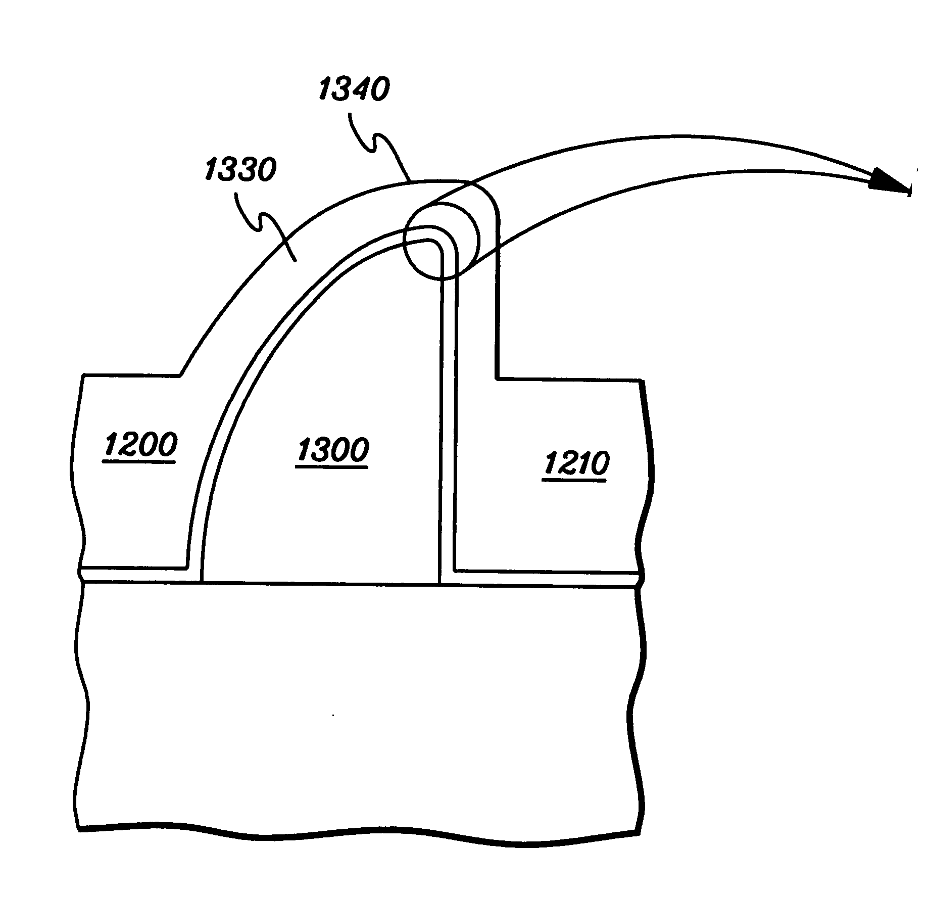
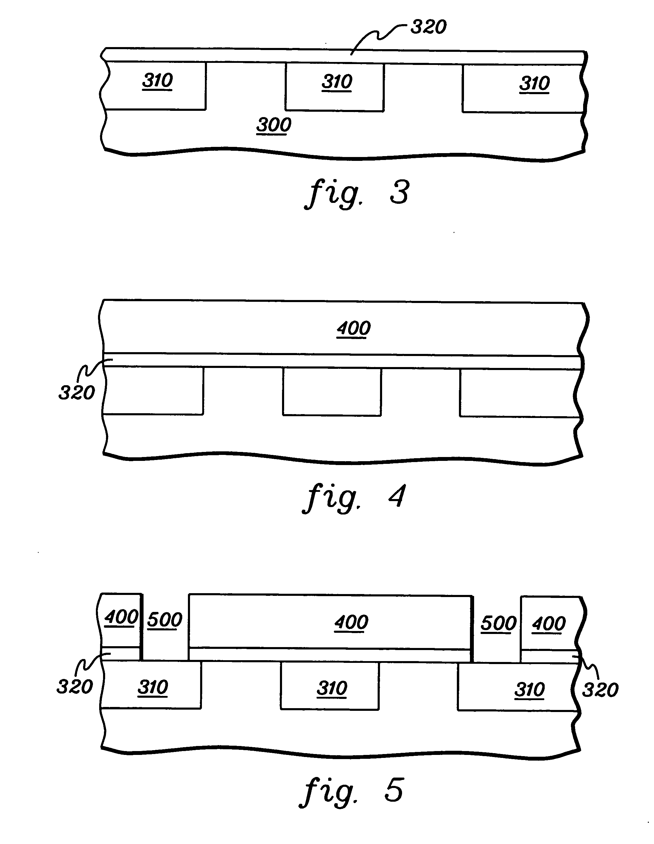
[0038] Recently developed e-fuse structures take advantage of electro-migration (EM) effects to overcome some of the above-noted problems of achieving scaling of programming voltage. The EM effect, caused by a positive divergence of the ionic flux, leads to an accumulation of vacancies, forming voids in the metal. Voids are formed inside of the metal conductors due to metal ion movement caused by momentum transfer from the electron flux at high current density. The void growth rate is a function of both temperature and current density, and therefore, the site having the smallest cross-sectional area in an interconnect tends to form voids first. Thus, it is advantageous to somehow increase the local current density in the fuse element.

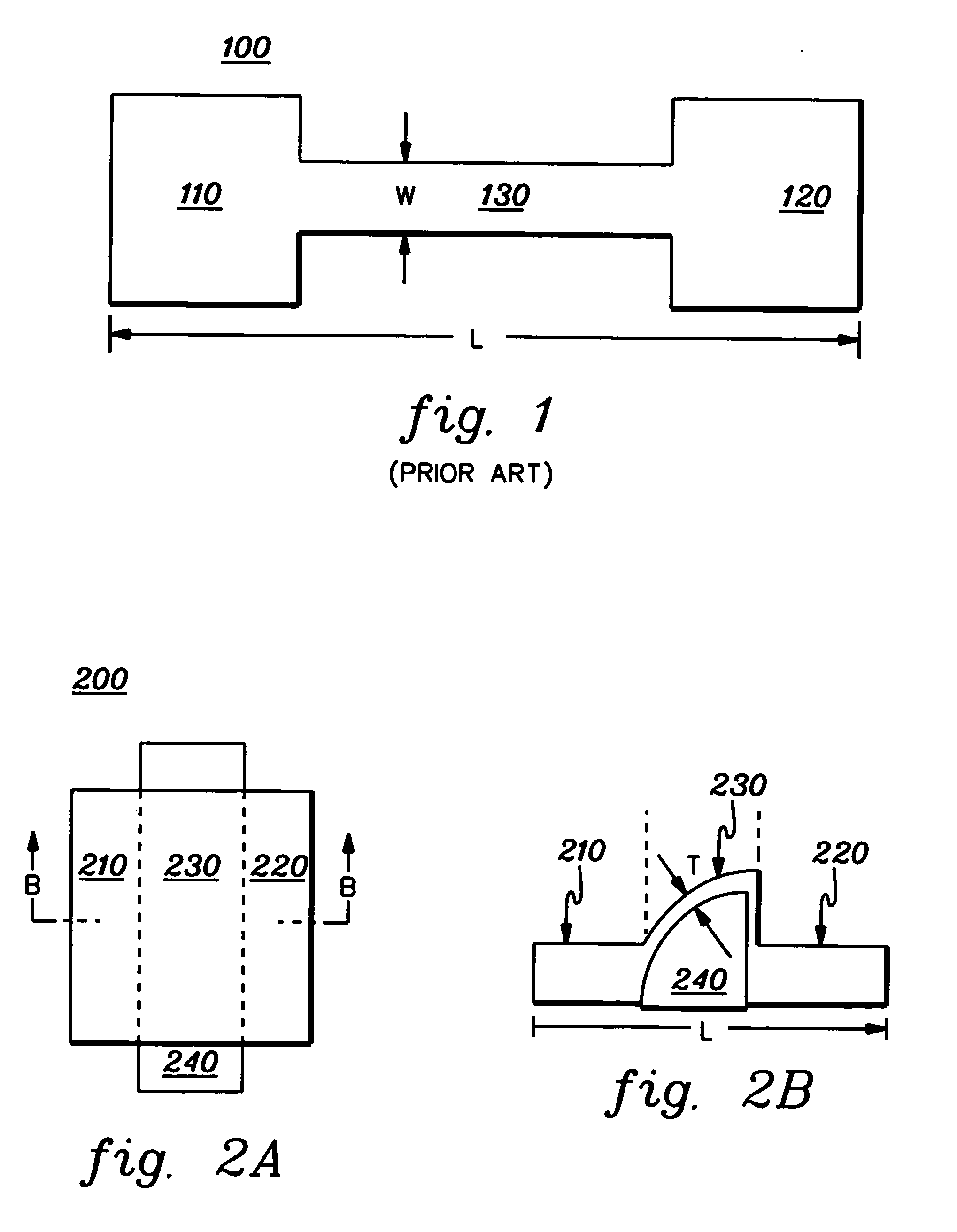
[0039] One approach to increasing local current density is depicted in FIG. 1, wherein the plan view layout of the illustrated electronic fuse 100 is a two-dimensional “dog-bone” shape. Fuse 100, which employs in-plane dimensional differences to locate...


PUM

PropertyMeasurementUnit
Lengthaaaaaaaaaa
Radiusaaaaaaaaaa
Electric potential / voltageaaaaaaaaaa

Abstract

An electronic fuse for an integrated circuit and a method of fabrication thereof are presented. The electronic fuse has a first terminal portion and a second terminal portion interconnected by a fuse element. The fuse element has a convex upper surface and a lower surface with a radius of curvature at a smallest surface area of curvature less than or equal to 100 nanometers. Fabricating the electronic fuse includes forming an at least partially freestanding dielectric spacer above a supporting structure, and then conformably forming the fuse element of the fuse over at least a portion of the freestanding dielectric spacer, with the fuse element characterized as noted above. The dielectric spacer may remain in place as a thermally insulating layer underneath the fuse element, or may be removed to form a void underneath the fuse element.

Description

CROSS-REFERENCE TO RELATED APPLICATIONS [0001] This application contains subject matter which related to the subject matter of the following co-filed, commonly assigned applications, each of which is hereby incorporated herein by reference in its entirety: [0002]“Electrically Programmable Fuse Structures with Terminal Portions Residing at Different Heights, and Methods of Fabrication Thereof”, by Hovis et al., U.S. Ser. No. ______, co-filed herewith (Attorney Docket No.: ROC920050384US1); [0003]“Electrically Programmable π-Shaped Fuse Structures and Methods of Fabrication Thereof”, by Booth et al., U.S. Ser. No. ______, co-filed herewith (Attorney Docket No. ROC920050386US1); and [0004]“Electrically Programmable Fuse Structures with Narrowed Width Regions Configured to Enhance Current Crowding and Methods of Fabrication Thereof”, by Booth et al., U.S. Serial No., co-filed herewith (Attorney Docket No.: ROC920050387US1).TECHNICAL FIELD [0005] The present invention relates in general ...

Claims


Application Information

Patent Timeline
IPC IPC(8): H01H85/04
CPCY10T29/49107H01L23/5256H01L2924/0002H01L2924/00
Inventor HSU, LOUIS LU-CHENMANDELMAN, JACK A.TONTI, WILLIAM R.YANG, CHIH-CHAO
Owner IBM CORP
Why Eureka
Try Eureka