
Conductive Member for Non-Contact Type Data Carrier and Method and Device for Manufacturing the Same

a technology of non-contact type and data carrier, which is applied in the direction of instruments, paper/cardboard articles, chemistry apparatus and processes, etc., can solve the problems of defective punching, reduced performance of antenna and the like, increased material used for the layered body, etc., and achieves smooth removal, and improved antenna and the like characteristics.

Active Publication Date: 2007-09-20
DAI NIPPON PRINTING CO LTD
View PDF7 Cites 10 Cited by
  • Summary
  • Abstract
  • Description
  • Claims
  • Application Information

AI Technical Summary

Benefits of technology

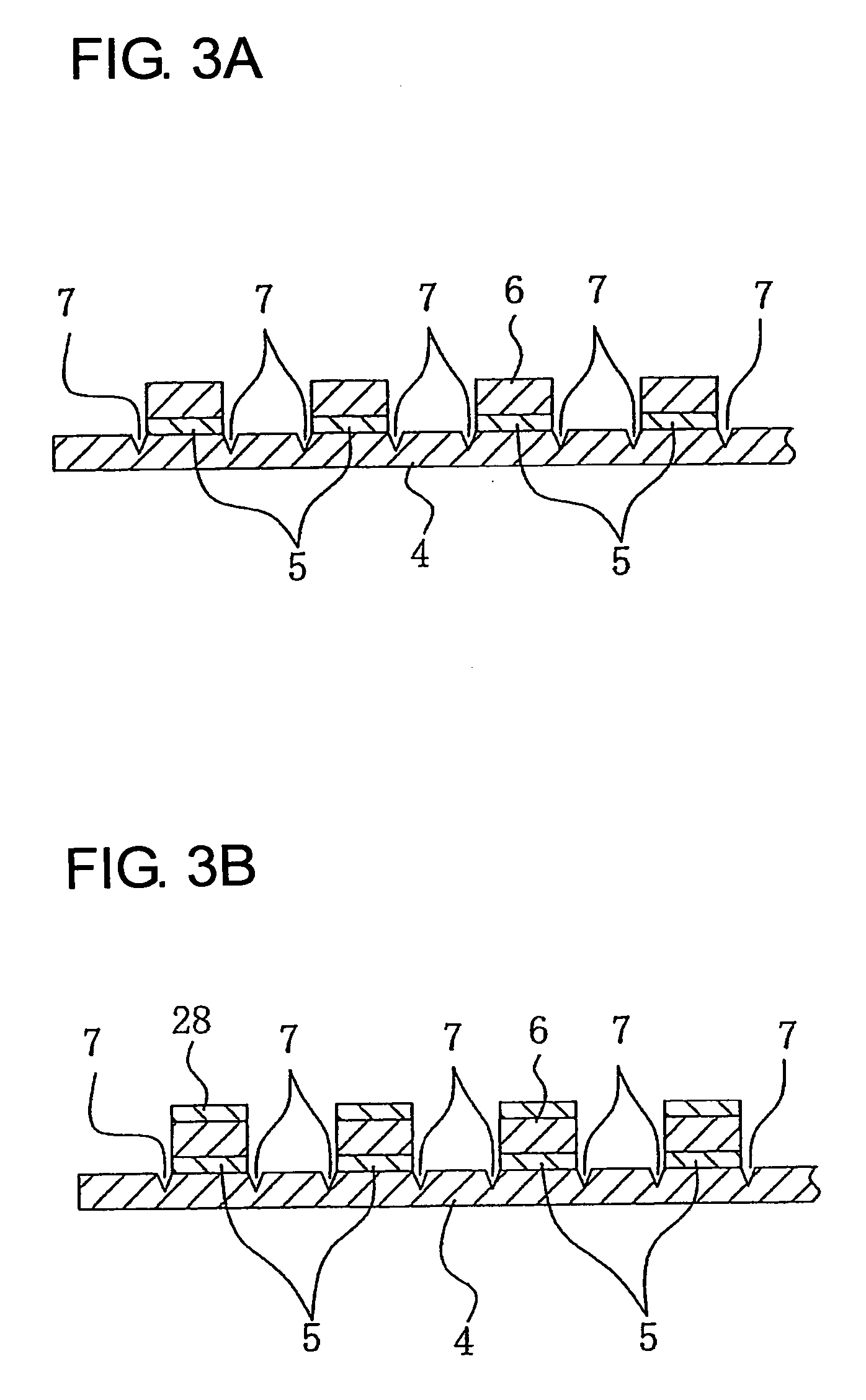
[0032] According to claim 2 of the invention, the conductive member for a non-contact type data carrier according to claim 1 of the invention has a configuration in which a slit (7) cutting the conductive layer (6) is formed on the base material (4) along the outline of the conductive layer (6). Accordingly, the pattern of the conductive layer (6) is neatly formed by the slit (7) to improve the electric performance of the conductive layer (6).
[0050] According to claim 20 of the invention, the device for manufacturing a conductive member for a non-contact type data carrier according to claim 17 of the invention has a configuration in which the separating means which separates the unnecessary portion (6b) of the conductive layer (6) from the base material (4) has sucking means (39) which sucks the unnecessary portion (6b) of the conductive layer (6), and a nozzle (40) which shoots gas to between the unnecessary portion (6b) of the conductive layer (6) and the base material (4). Accordingly, it is obvious that the unnecessary portion (6b) of the conductive layer (6) may be smoothly removed, and the device structure for separating may be simplified.

Problems solved by technology

According to the conventional manufacturing methods, there is a problem that the punching blade of the metal foil and the metal mold are required to be made so that the patterns are in accurate accordance with each other and operations are in exact synchronization to obtain an accurate pattern of an antenna and the like.
There is another problem that, as a layered body is required to be used as a material, a material used for the layered body is increased.
Moreover, a second problem is that there is a possibility that air bubbles and the like exist between the metal foil and the base material, the edge of the pattern is curled from the base material after pattern punching for the antenna and the like, and the metal foil has a wavy surface.
The second problem causes reduction in the performance of the antenna and the like.
A third problem is a possibility that, when the metal foil is punched with the punching blade, there is caused defective punching, insufficient melting of the bonding agent, or inconsistencies in pressing.
The third problem causes unreliable forming of the pattern of the antenna and the like.
A fourth problem is that, when the metal foil is bonded to the base material, a bonding agent, which should not be heated is required to be used in some cases.

Method used


Image

  • Conductive Member for Non-Contact Type Data Carrier and Method and Device for Manufacturing the Same
  • Conductive Member for Non-Contact Type Data Carrier and Method and Device for Manufacturing the Same
  • Conductive Member for Non-Contact Type Data Carrier and Method and Device for Manufacturing the Same

Examples


embodiment 1

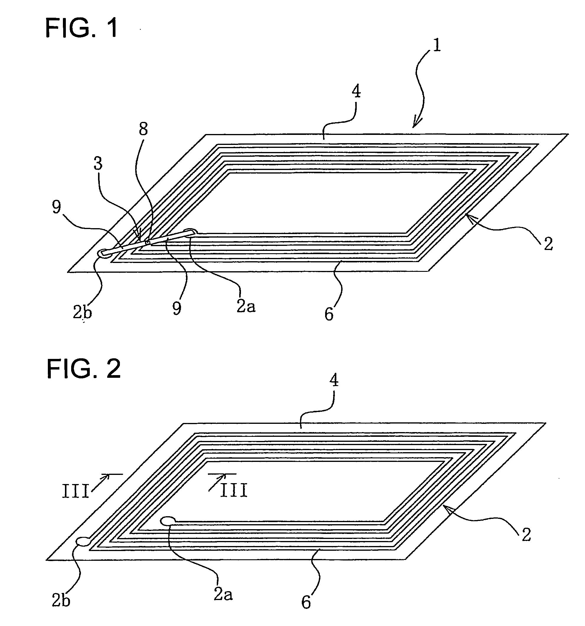
[0115] A wireless tag 1 shown in FIG. 1 is made, using an antenna 2 as a conductive member as shown in FIG. 2 for a non-contact type data carrier and an interposer 3 as shown in FIG. 4 as a conductive member for a non-contact type data carrier. As shown in FIG. 1, the ends 2a and 2b of the antenna 2 are electrically connected to each other through the interposer 3, and the surface of the whole of the wireless tag 1 is covered with a not-shown protective layer such as a resin film.

[0116] The antenna 2 has a layer configuration as shown in FIG. 3(A). That is, a thermoplastic bonding agent layer 5 is printed on a sheet-like base material 4 made of paper, resin and the like in the same pattern as a spiral pattern of the antenna 2, and a conductive layer 6 comprising metal foil of aluminum, copper, copper alloy, phosphor bronze, SUS and the like or alloy foil is heated and bonded to the above thermoplastic bonding agent layer 5 in the spiral pattern of the antenna 2. Here, the antenna h...

embodiment 2

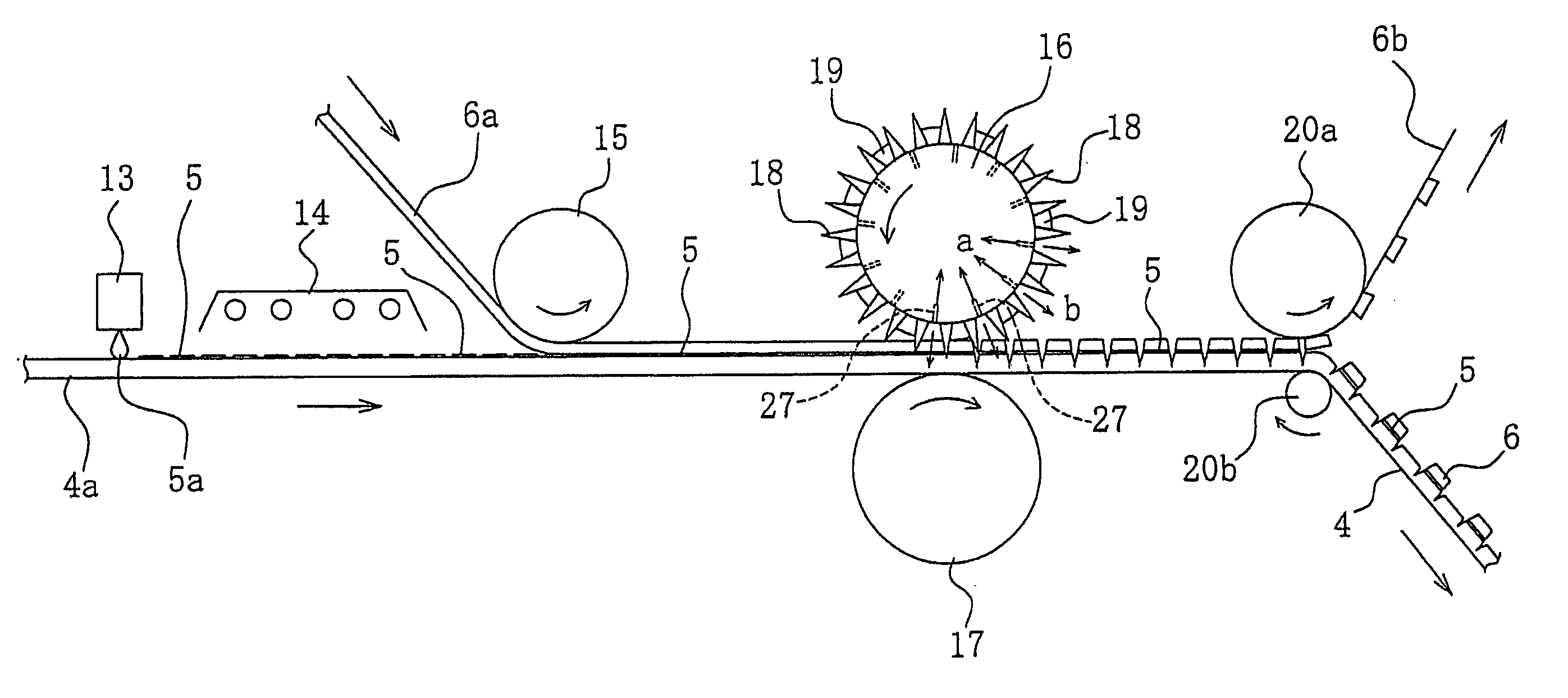
[0135] As shown in FIG. 7, the present embodiment 2 has a configuration in which the processing cylinder 16 in the embodiment 1 is separated to two cylinders 16a and 16b, which are arranged along the running direction of a continuous body 4a of a base material 4 and a continuous body 6a of metal foil as a conductive layer 6. The cylinder 16a on the upstream side is a heating cylinder on the peripheral surface of which there are formed heat transfer bodies 19 which are formed in a convex state and has a heating pattern corresponding to the pattern of an antenna 2. The heat transfer body 19 is formed of rubber, heat-resistant resin and the like, which have cushion and heat transfer performances. Moreover, the cylinder 16a may be also made by patterning with a metal roll. The cylinder 16b on the downstream side is a punching cylinder, and punching blades 18 corresponding to the pattern of the antenna 2 are formed on the peripheral surface thereof. The heating cylinder 16a is arranged o...

embodiment 3

[0139] The present embodiment 3 has a configuration, different from that of the embodiment 1, in which a flat plate 21 as a flat blade knife of a flat press machine is substituted for the processing cylinder 16, and a pedestal 22 is substituted for the receiving roller 17, as shown in FIG. 8.

[0140] In this case, a continuous body 4a of a base material 4 and a continuous body 6a of metal foil as a conductive layer 6 are intermittently fed at a constant pitch to between a processing flat plate 21 and a pedestal 22, and the processing flat plate 21 is reciprocally moved up and down to the pedestal 22. Then, the continuous body 6a of the metal foil as the conductive layer 6 is punched in the pattern of an antenna 2 at each reciprocal movement, and is pressed onto a melted thermoplastic bonding agent layer 5 on the continuous body 4a of the base material 4. Thereafter, the continuous body 4a of the base material 4 and the continuous body 6a of the metal foil as the conductive layer 6 ar...


PUM

PropertyMeasurementUnit
conductiveaaaaaaaaaa
electric performanceaaaaaaaaaa
durabilityaaaaaaaaaa

Abstract

A conductive member for a non-contact type data carrier such as a wireless tag is simply and cheaply manufactured. A method for manufacturing a conductive member for a non-contact type data carrier comprises: a printing process during which, while a base material (4) is run, a bonding agent layer (5) is printed in a predetermined pattern on the surface thereof, and is dried; a bonding process during which a conductive layer (6) is laminated on the surface of the bonding agent layer (5) for heating and bonding; a punching process during which the conductive layer (6) is punched in the above-described pattern on the base material (4); and a separating process during which an unnecessary portion (6b) of the conductive layer (6) is separated from the base material (4). Accordingly, a conventional multilayered laminated sheet is not required to realize reduction in the material.

Description

TECHNOLOGICAL FIELD [0001] The present invention relates to a conductive member for a non-contact type data carrier such as an antenna, an interposer, and a bridge, and a method and a device for manufacturing the same. BACKGROUND ART [0002] A conductive member for a non-contact type data carrier such as an antenna is used to make, for example, a wireless tag used for a commodity. [0003] When an antenna as a conductive member for a non-contact type data carrier is formed in a predetermined pattern, the antenna has been manufactured by etching after forming a resist pattern on a metal layer such as an aluminum layer and a copper one laminated on a base material. [0004] Moreover, there has been another method by which the antenna is directly formed, using a punching blade. According to the method, there is prepared a layered body obtained by applying a thermoplastic bonding agent on metal foil after the metal foil is bonded to a carrier such as a plastic film through a peeling layer an...

Claims


Application Information

Patent Timeline
Patent Type & Authority Applications(United States)
IPC IPC(8): H05K3/20G06K19/00H05K3/04
CPCH05K3/041H05K3/046H05K2201/0355H05K2203/0522Y10T29/49128Y10T29/49163Y10T156/1054Y10T29/49156Y10T29/49126H05K2203/1545
Inventor NAKANISHI, YUKISAKATA, HIDETOIGARASHI, AKIHIKO
Owner DAI NIPPON PRINTING CO LTD
Learn More