Magnetic tunnel junction patterning using Ta/TaN as hard mask

Active Publication Date: 2007-09-20
TAIWAN SEMICON MFG CO LTD
View PDF15 Cites 40 Cited by
  • Summary
  • Abstract
  • Description
  • Claims
  • Application Information

AI Technical Summary

Benefits of technology

[0017] A second object of the present invention is to provide a hard mask structure that does not have the disadvantageous properties of prior art hard masks that also serve as capping layers, such as poor adhesion of dielectric layers and mask oxidation.
[0018] A third object of the present invention is to provide a hard mask structure that can be used to precisely define an MTJ pattern and, thereby, precisely define the size and shape of the resulting cell.
[0019] A fourth object of the present invention is to provide such a hard mask structure that can, itself, be easily patterned within the fabrication process steps.
[0020] A fifth object of this invention is to provide an MTJ MRAM cell capped by a non-oxidized layer that has served as a hard mask for the patterning of said cell and surrounded by insulating layers exhibiting good adhesion and, therefore, effective planarization.
[0021] These objects will be met by use of a hard mask that is formed by patterning a

Problems solved by technology

One of the critical challenges in MRAM technology is the patterning of the MTJ stack materials to form an MRAM cell.
Because the MTJ stack includes a very thin tunneling barrier layer, typically a layer of AlOx or MgO approximately 10 to 20 angstroms in thickness, shorting or shunting of the current around the junction is a critical problem.
Unfortunately, the IBE has several disadvantages, including non-selectivity, re-deposition of etched materials and the production of a tapered tail profile on the lateral etched edges of the stack.
Among these disadvantages is the poor adhesion of Ta to dielectric layers, such as layers of SiN, SiO2, F-doped SiOx and C-doped SiO2 that are applied onto and around the patt

Method used


Image

  • Magnetic tunnel junction patterning using Ta/TaN as hard mask
  • Magnetic tunnel junction patterning using Ta/TaN as hard mask
  • Magnetic tunnel junction patterning using Ta/TaN as hard mask

Examples


Embodiment Construction

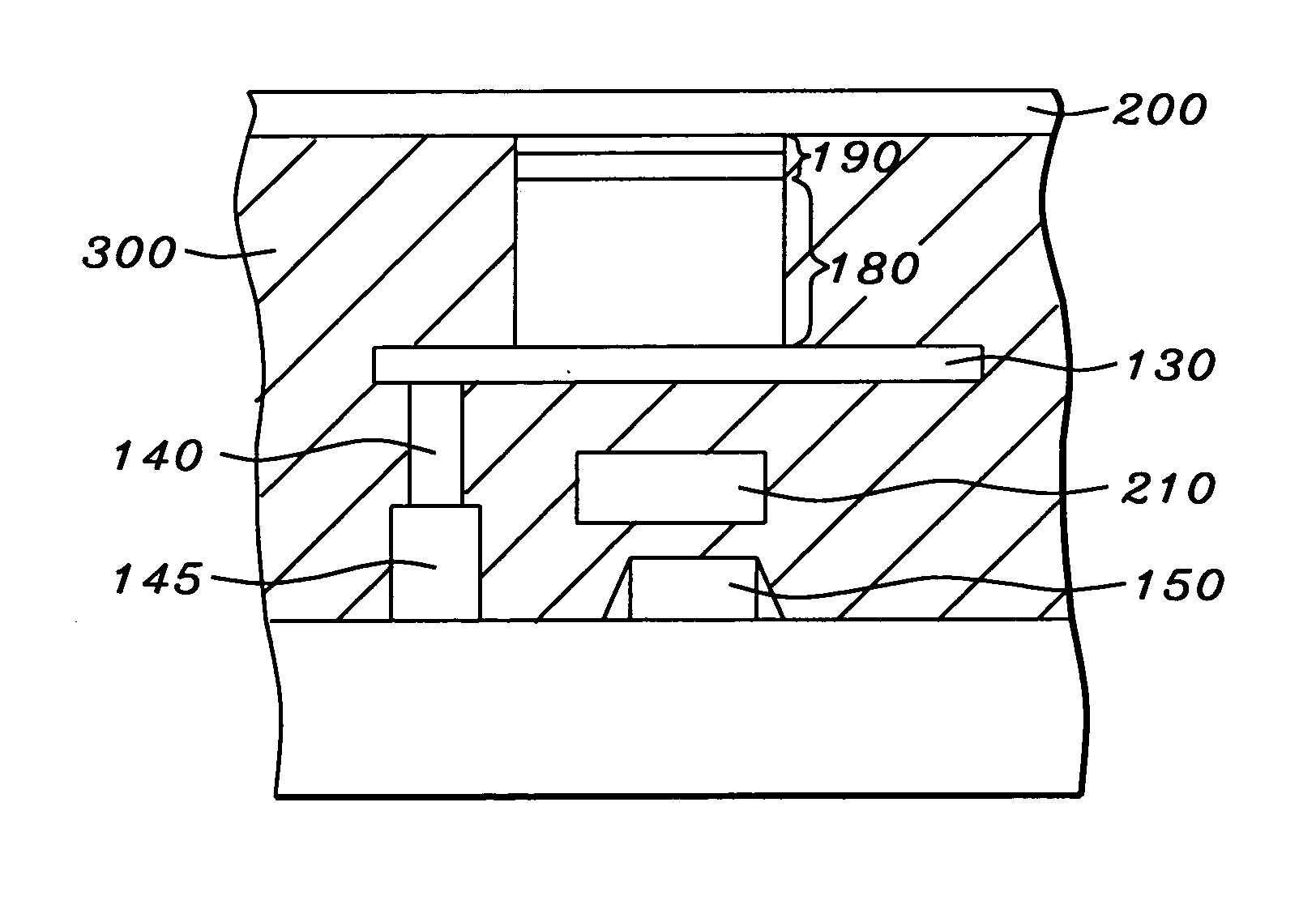
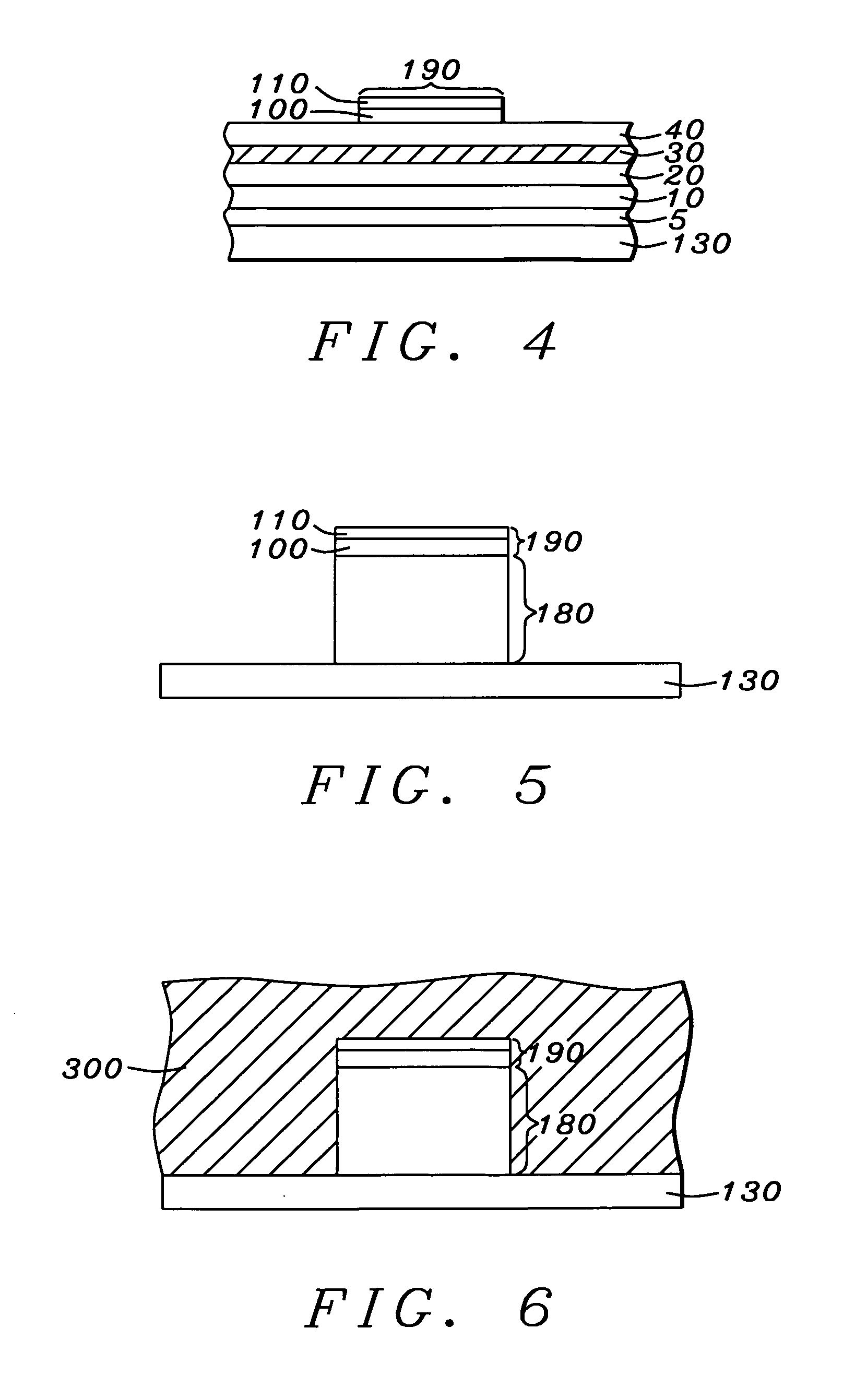
[0029] The preferred embodiment of the present invention is the formation and use of a bilayer Ta / TaN hard mask, that is used to pattern an MTJ stack using a reactive ion etch (RIE) and to produce, thereby, an MTJ cell suitable for use in an MRAM array. The patterned cell so produced is capped by the Ta / TaN mask, providing a TaN upper surface that has good adhesion to the surrounding dielectric layers and further providing a non-oxidized and low resistance Ta layer immediately adjacent to and contacting the upper surface of the MTJ cell.

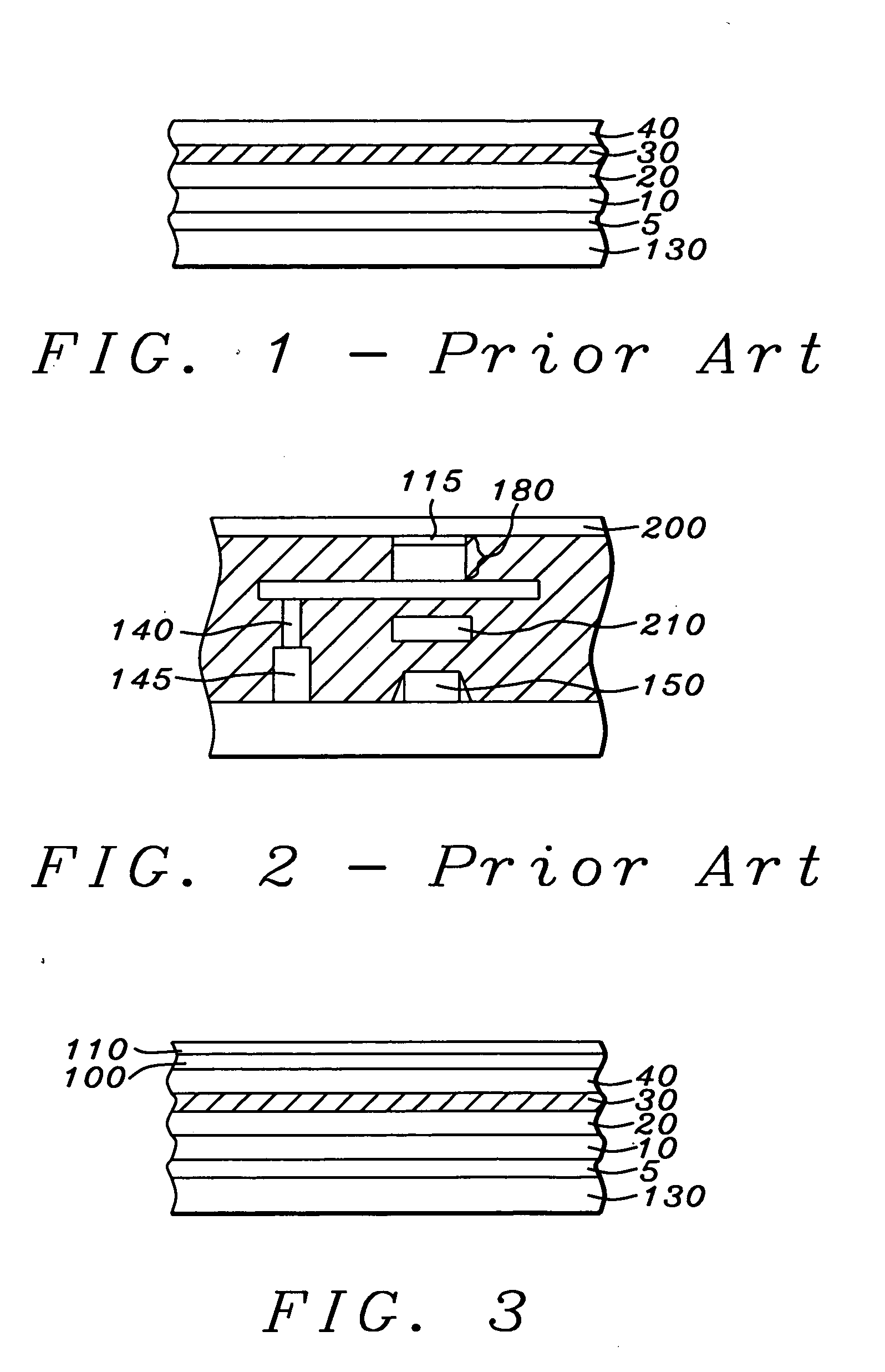
[0030] Referring to FIG. 3, there is shown an MTJ stack of the type shown in FIG. 1 (all layers and designating numerals being identical to those described in FIG. 1) on which is being formed a Ta / TaN bilayer (100), (110), to be patterned and used as the mask of the present invention. The lower layer (100) is a layer of Ta deposited on the upper ferromagnetic free layer (40) of the stack by any of the prior art deposition methods including PVD, CVD,...


PUM


Abstract

An MTJ MRAM cell is formed by using a reactive ion etch (RIE) to pattern an MTJ stack on which there has been formed a bilayer Ta/TaN hard mask. The hard mask is formed by patterning a masking layer that has been formed by depositing a layer of TaN over a layer of Ta on the MTJ stack. After the stack is patterned, the TaN layer serves at least two advantageous purposes: 1) it protects the Ta layer from oxidation during the etching of the stack and 2) it serves as a surface having excellent adhesion properties for a subsequently deposited dielectric layer.

Description

BACKGROUND OF THE INVENTION [0001] 1. Field of the Invention [0002] This invention relates to the fabrication of a magnetic tunneling junction (MTJ) cell and more particularly to the nature of the etching processes used in the fabrication. [0003] 2. Description of the Related Art [0004] The magnetic tunneling junction (MTJ) device, is a form of giant magnetoresistive (GMR) device in which the relative orientation of uni-directional magnetic moments in parallel, vertically separated upper and lower magnetized layers, controls the flow of spin-polarized electrons tunneling through a very thin dielectric layer (the tunneling barrier layer) formed between those layers. When injected electrons pass through the upper layer they are spin polarized by interaction with the magnetic moment of that layer. The probability of such an electron then tunneling through the intervening tunneling barrier layer into the lower layer then depends on the availability of states within the lower electrode t...

Claims


Application Information

Patent Timeline
IPC IPC(8): H01L29/82H01L21/00
CPCH01L43/12H01L43/08H10N50/01H10N50/10
Inventor TORNG, CHYU-JIUHCAO, WEIKO, TERRY
Owner TAIWAN SEMICON MFG CO LTD
Why Eureka
Try Eureka