Nitride semiconductor single crystal substrate, and methods of fabricating the same and a vertical nitride semiconductor light emitting diode using the same

a technology of nitride semiconductor and single crystal substrate, which is applied in the field of nitride single crystal substrate, can solve the problems of complex process, complex process, and single crystal defects, and achieve the effect of improving crystallinity

Active Publication Date: 2007-09-20
SAMSUNG ELECTRONICS CO LTD
View PDF19 Cites 7 Cited by
  • Summary
  • Abstract
  • Description
  • Claims
  • Application Information

AI Technical Summary

Benefits of technology

[0018]The lower region has a thickness ranging from 100 μm to 500 μm. This assures superior crystallinity and simplifies a lapping process. Also, preferably, the upper region has a thickness ranging from 10 μm to 100 μm.
[0026]Preferably, the first and second nitride single crystal layers are grown by Hydride Vapor Phase Epitaxy which ensures high speed growth.
[0032]Preferably, the step of sequentially growing the active layer and the second conductive nitride semiconductor layer includes growing the first conductive nitride semiconductor layer before growing the active layer. Preferably, the active layer and the second conductive nitride semiconductor layer are sequentially grown by Metal Organic Vapor Phase Epitaxy which beneficially ensures better crystallinity.

Problems solved by technology

This causes stress to an interface between the sapphire substrate and a nitride gallium single crystal, thereby resulting in lattice defects and cracks in the single crystal.
However, in reality, even with use of the nitride single crystal substrate, there is a difficulty in fabricating the vertical light emitting device.
Otherwise, it entails a complicated process since the nitride single crystal substrate should be entirely removed by mechanical polishing to fabricate a vertical light emitting device.
Yet, higher concentration of impurities in the nitride single crystal increases stress in the single crystal and accordingly defect density, thereby leading to degradation of crystal quality such as decline in carrier mobility.
Such doping with specific impurities may inflict cracks on a large-scale substrate which is manufactured.

Method used


Image

  • Nitride semiconductor single crystal substrate, and methods of fabricating the same and a vertical nitride semiconductor light emitting diode using the same
  • Nitride semiconductor single crystal substrate, and methods of fabricating the same and a vertical nitride semiconductor light emitting diode using the same
  • Nitride semiconductor single crystal substrate, and methods of fabricating the same and a vertical nitride semiconductor light emitting diode using the same

Examples


Embodiment Construction

[0038]Exemplary embodiments of the present invention will now be described in detail with reference to the accompanying drawings.

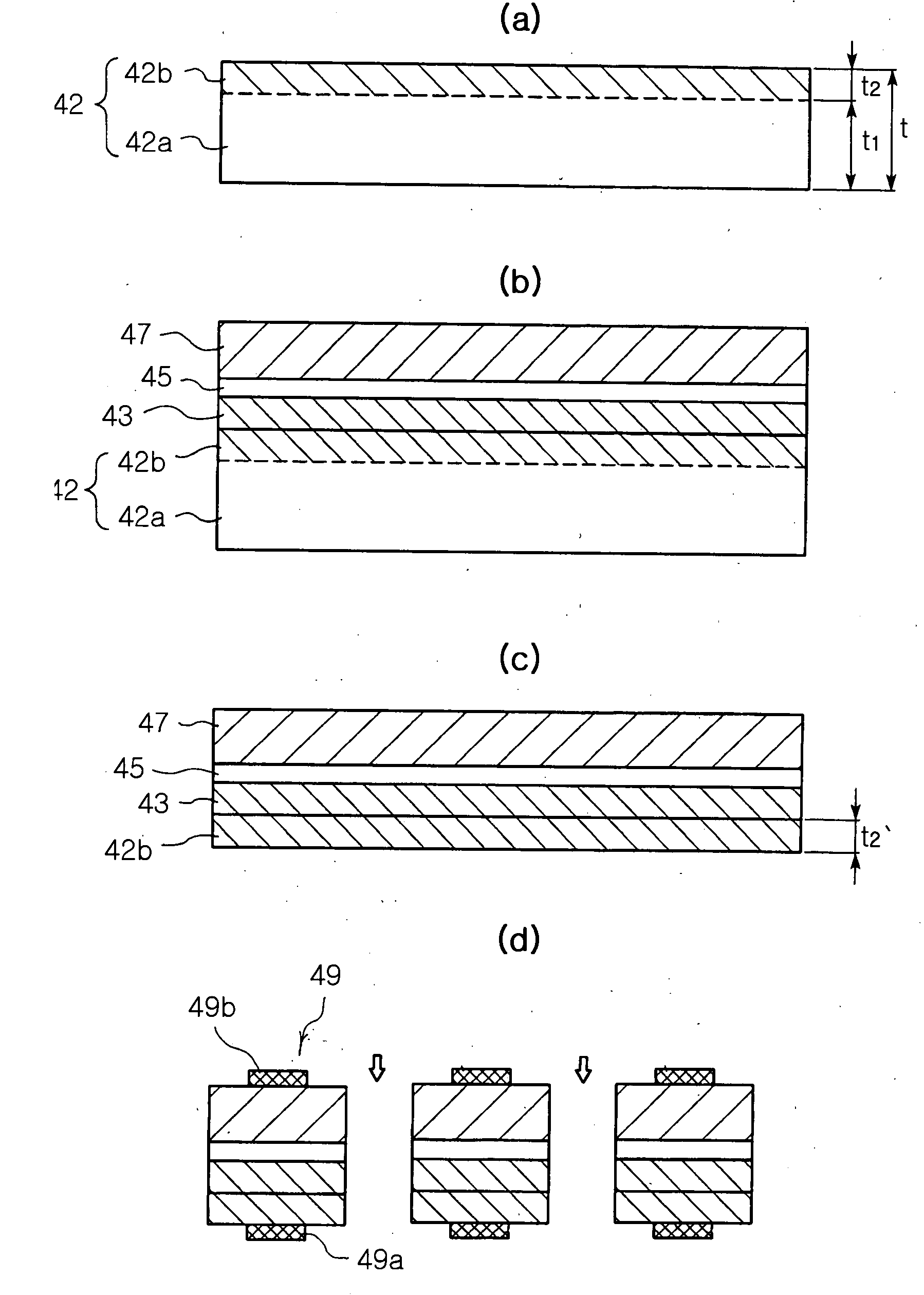
[0039]FIG. 2a is a side cross-sectional view illustrating a nitride single crystal substrate according to a first aspect of the invention.

[0040]As shown in FIG. 2a, the nitride single crystal substrate 22 of the invention includes upper and lower regions 22b and 22a along a thickness direction. The upper region 22b is highly doped and the lower region 22a is intentionally un-doped. The nitride single crystal substrate 22 is made of a material having a composition expressed by AlxInyGa(1-x-y)N, where 0≦x≦1, 0≦y≦1, and 0≦x+y≦1. Here, the upper region 22b may have a composition identical to that of the lower region 22a. However, the upper region 22b has a doping concentration at least five times greater than that of the lower area 22a. The upper region 22b is doped to be sufficiently conductive. In contrast, the lower region 22b may be intentionally un-doped....


PUM

PropertyMeasurementUnit
thicknessaaaaaaaaaa
thicknessaaaaaaaaaa
thicknessaaaaaaaaaa

Abstract

A nitride semiconductor single crystal substrate, a manufacturing method thereof and a method for manufacturing a vertical nitride semiconductor device using the same. According to an aspect of the invention, in the nitride semiconductor single crystal substrate, upper and lower regions are divided along a thickness direction, the nitride single crystal substrate having a thickness of at least 100 μm. Here, the upper region has a doping concentration that is five times or greater than that of the lower region. Preferably, a top surface of the substrate in the upper region has Ga polarity. Also, according to a specific embodiment of the invention, the lower region is intentionally un-doped and the upper region is n-doped. Preferably, each of the upper and lower regions has a doping concentration substantially identical in a thickness direction.

Description

CLAIM OF PRIORITY[0001]This application claims the benefit of Korean Patent Application No. 2006-24918 filed on Mar. 17, 2006 in the Korean Intellectual Property Office, the disclosure of which is incorporated herein by reference.BACKGROUND OF THE INVENTION[0002]1. Field of the Invention[0003]The present invention relates to a nitride single crystal substrate, and more particularly, to a nitride single crystal substrate capable of facilitating a manufacturing process of a light emitting device and a vertical nitride light emitting device using the same.[0004]2. Description of the Related Art[0005]In general, a group III nitride semiconductor emits a wide range of light from a visible light to an ultraviolet ray. The group III nitride semiconductor has been greatly highlighted as an optical device material for realizing bluish green light.[0006]Typically, a nitride single crystal has been produced on a heterojunction substrate by a vapor growth method such as Metal Organic Vapor Phas...

Claims


Application Information

Patent Timeline
Patent Type & Authority Applications(United States)
IPC IPC(8): H01L29/12H01L33/32
CPCH01L21/0237H01L21/0242H01L21/02458H01L21/0254H01L33/0075H01L21/0262H01L21/02664H01L29/2003H01L21/02576A47K10/32A47K10/42A47K2010/3233
Inventor KIM, CHEOL KYURYU, YUNG HOLEE, SOO MINYANG, JONG INKIM, TAE HYUNG
Owner SAMSUNG ELECTRONICS CO LTD
Why Eureka
Try Eureka