
Light emitting device having vertical structure and mehod for manufacturing the same

a technology vertical structures, which is applied in the direction of semiconductor/solid-state device manufacturing, semiconductor devices, electrical devices, etc., can solve the problems of high production costs, limited lateral or vertical structure of available led devices manufactured using sapphire substrates, and inability to practically produce pure green light. , to achieve the effect of improving the light extraction efficiency of light emitting devices, improving the crystalline quality of thin films, and high efficiency

Active Publication Date: 2007-09-27
LG ELECTRONICS INC +2
View PDF4 Cites 35 Cited by
  • Summary
  • Abstract
  • Description
  • Claims
  • Application Information

AI Technical Summary

Benefits of technology

[0031]An object of the present invention is to provide a light emitting device having a vertical structure and a method for manufacturing the same which can achieve a high-brightness and high-efficient light emitting device by adapting a photonic crystal structure capable of improving light extraction efficiency to the light emitting device.
[0032]Another object of the present invention is to provide a light emitting device having a vertical structure and a method for manufacturing the same which can improve crystalline quality of a thin film by growing the thin film selectively on a light extraction structure formed in a specific shape.
[0033]Yet another object of the present invention is to provide a light emitting device having a vertical structure and a method for manufacturing the same which can improve efficiency of a light emitting device by controlling strain in a thin film.

Problems solved by technology

Since GaP is an indirect transition material causing degradation in efficiency, the green LEDs fabricated using this material cannot practically produce light of pure green.
Despite the rapid advancement in technologies of GaN-based semiconductor devices, the fabrication of GaN-based devices suffers from a great disadvantage of high-production costs.
This disadvantage is closely related to difficulties associated with growing of a GaN thin film (epitaxial layer) and subsequent cutting of finished GaN-based devices.
Meanwhile, since sapphire is an insulating material, available LED devices manufactured using a sapphire substrate (or other insulating substrates) are practically limited to a lateral or vertical structure.
However, the method using the photonic crystal is not applied to the mass production technologies of the light emitting devices until now.
However, this method has a limitation in the improvement of the light extraction efficiency, because of basically low electrical features of the p-type GaN layer 4, a thin thickness and degradation of the electrical features by the etching.
However, basically low electric conductivity of the p-type GaN layer, low crystalline quality and degradation of electrical features by the etching make the growth of the p-type GaN layer on the substrate impossible.
However, because of low electrical features of the p-type GaN layer, this method also has problem that resistance at a junction portion is increased and resultantly operating voltage of the device is increased.
However, because the metal plate is not stable sufficiently in the etching process of the thin film layer, it is difficult to perform the etching process, and productivity is low.

Method used


Image

  • Light emitting device having vertical structure and mehod for manufacturing the same
  • Light emitting device having vertical structure and mehod for manufacturing the same
  • Light emitting device having vertical structure and mehod for manufacturing the same

Examples


first embodiment

[0068]Hereinafter, a first embodiment of the present invention will be described with reference to FIGS. 3 to 8.

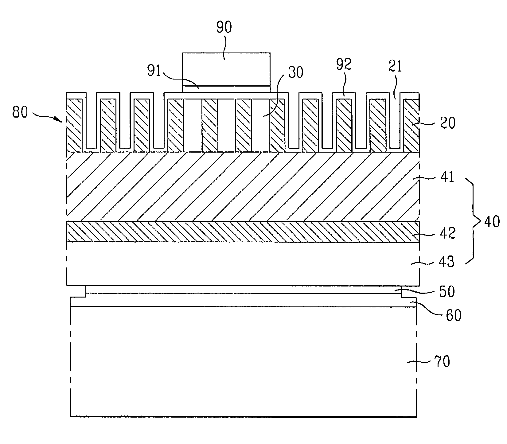
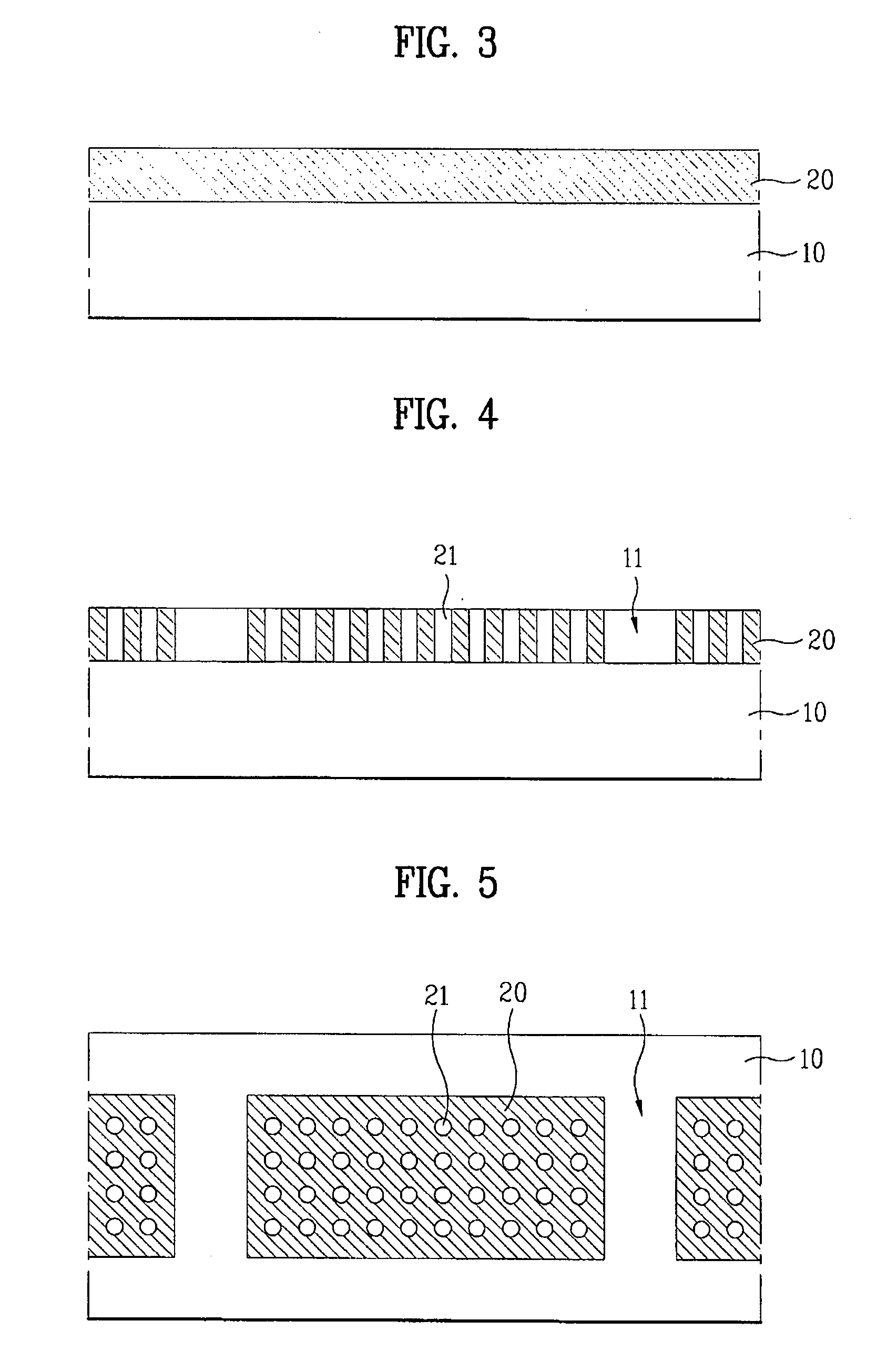
[0069]In order to form a light extraction layer on a substrate, as shown in FIG. 3, a substrate 10 is subjected to surface treatment through a wet treatment process or a dry treatment process, and a GaN semiconductor layer 20 is formed on the substrate 10 by using a common semiconductor thin film growing device.

[0070]The substrate 10 may be made of material selected from the group consisting of sapphire, silicon (Si), zinc oxide (ZnO), silicon carbide (SiC), and a combination thereof. Preferably, the GaN semiconductor layer 20 is grown to a thickness of 0.3 to 5 μm. The GaN semiconductor layer 20 may be formed using n-type GaN material.

[0071]As shown in FIG. 4, holes 21 with regular period and pattern are formed on the GaN semiconductor layer 20 by using a patterning process and an etching process. The planar shape of the substrate 10 and the GaN semiconductor layer 20 wit...

second embodiment

[0121]Hereinafter, a second embodiment of the present invention will be described with reference to FIGS. 10 to 12.

[0122]In order to form a light extraction layer on a substrate, as shown in FIG. 10, a substrate 100 is subjected to surface treatment through a wet treatment process or a dry treatment process. The substrate 100 may be made of material selected from the group consisting of sapphire, silicon (Si), zinc oxide (ZnO), silicon carbide (SiC), and a combination thereof.

[0123]As shown in FIG. 11, a plurality of columns 200 of dielectric material are formed on the substrate 100. The columns 200 of dielectric material have a cross section of a circular shape or a polygonal shape like a rectangle, a hexagon, etc.

[0124]The columns 200 of dielectric material may be made of oxide or nitride, and more particularly, silicon dioxide (SiO2) or silicon nitride (SiN).

[0125]The columns 200 of dielectric material may be formed through a patterning process or an etching process. In other wor...

third embodiment

[0127]Hereinafter, a third embodiment of the present invention will be described with reference to FIGS. 13 to 17.

[0128]As shown in FIG. 13, a GaN semiconductor thin film 110 is grown on a substrate 100 by using a common semiconductor thin film growing device, and columns 200 of dielectric material are formed on the GaN semiconductor thin film 110.

[0129]At this time, the GaN semiconductor thin film 110 may be formed only on the regions where the unit device is formed. Alternatively, the semiconductor thin film 110 may be firstly formed on the overall surface, and a portion of the semiconductor thin film positioned on the unit-device division regions may be secondarily etched to be removed.

[0130]It is preferable to set the thickness of the thin film 110 to be 0.001 to 5 μm. The thin film 110 may function as a buffer layer on the substrate 100.

[0131]As shown in FIG. 14, the columns 200 of dielectric material are formed on the GaN semiconductor thin film 110.

[0132]FIG. 15 illustrates t...


PUM


Abstract

A light emitting device having a vertical structure and a method for manufacturing the same, which are capable of increasing light extraction efficiency, are disclosed. The method includes forming a light extraction layer on a substrate, forming a plurality of semiconductor layers on the light extraction layer, forming a first electrode on the semiconductor layers, forming a support layer on the first electrode, removing the substrate, and forming a second electrode on a surface from which the substrate is removed.

Description

[0001]This application claims the benefit of Korean Patent Application No. 10-2006-0025691, filed on Mar. 21, 2006 and Korean Patent Application No. 10-2006-0025692, filed on Mar. 21, 2006, which are hereby incorporated by references as if fully set forth herein.BACKGROUND OF THE INVENTION[0002]1. Field of the Invention[0003]The present invention relates to a light emitting device having a vertical structure, and more particularly, to a light emitting device having a vertical structure and a method for manufacturing the same which are capable of increasing light extraction efficiency.[0004]2. Discussion of the Related Art[0005]Light emitting diodes (LEDs) are well known as a semiconductor light emitting device which converts current to light, to emit light. Since a red LED using GaAsP compound semiconductor was commercially available in 1962, it has been used, together with a GaP:N-based green LED, as a light source in electronic apparatuses, for image display.[0006]The wavelength o...

Claims


Application Information

Patent Timeline
Patent Type & Authority Applications(United States)
IPC IPC(8): H01L29/06H01L33/32H01L33/42
CPCH01L2933/0083H01L33/20
Inventor JANG, JUN HOMOON, YONG TAE
Owner LG ELECTRONICS INC
Features
  • Generate Ideas
  • Intellectual Property
  • Life Sciences
  • Materials
  • Tech Scout
  • Unparalleled Data Quality
  • Higher Quality Content
  • 60% Fewer Hallucinations
Learn More