Fast method to model photoresist images using focus blur and resist blur

a technology of resist blur and focus blur, which is applied in the field of fast method to model photoresist images using focus blur and resist blur, can solve the problems of large cost incentive to do, feature size shrinkage well below half the wavelength of light (/2), and the model used within this opc software is difficult to adjust to actual processes, so as to achieve the effect of reducing the differences in the dimension of the patterned obj

Inactive Publication Date: 2007-09-27
GLOBALFOUNDRIES INC
View PDF2 Cites 12 Cited by
  • Summary
  • Abstract
  • Description
  • Claims
  • Application Information

AI Technical Summary

Benefits of technology

[0016] Bearing in mind the problems and deficiencies of the prior art, it is therefore an object of the present invention to provide an improved method for simulating and determining an image of a patterned object to be formed in a resist layer by a polychromatic lithographic projection system.
[0017] It is another object of the present invention to provide a method for simulating the effect of finite source bandwidth in polychromatic lithographic imaging systems that is practical for use with optical proximity correction modeling of object patterns.
[0018] A further object of the invention is to provide a method that improves accuracy and speed in simulating an image of a patterned object formed in a polychromatic lithographic projection system.
[0020] It is a further object of the present invention to provide a method for modifying an image of a patterned object in one or more polychromatic lithographic projection systems such that, when the spectral bandwidth of the illumination changes, control settings in a projection system may be adjusted to minimize the change in the dimensions of printed patterns.
[0026] The aforedescribed method may further be used to determine the images of the patterned object produced by a changed finite spectral bandwidth, and may include subsequently adjusting control settings in the lithographic projection system to minimize differences in dimension of the patterned objects formed in the resist layer by the changed spectral bandwidth.

Problems solved by technology

The accurate simulation of lithographic processes can be used to eliminate many experiments, and there is huge cost incentive to do this whenever possible.
Sub-100 nm features represent a significant challenge in the manufacture of ICs since such feature sizes approach the resolution limits of the lithographic imaging tools employed in IC fabrication.
The practical difficulty as feature sizes shrink well below half the wavelength of light (λ / 2) is not in avoiding a hard resolution limit, but rather in successfully printing the circuit patterns within an acceptable tolerance about the correct dimensions even as the exposing image departs substantially from an ideal binary pattern.
Unfortunately, the models used within this OPC software are difficult to adjust to actual processes because they contain many adjustable fitting parameters, and these parameters do not correspond to measurable physical quantities.
The OPC modeling software is frequently not accurate, and is too slow.
Narrow process margins make it necessary to optimize as many variables as possible during lithographic printing, and this optimization cannot be accomplished by trial-and-error or heuristic rules due to the complexity involved.
An important additional challenge arises when simulation is carried out for OPC, due to the enormous number of image calculations that OPC programs must carry out to correct the roughly 1 E8 features in state-of-the-art circuit masks.
Unfortunately, known methods for simulating the effect of finite source bandwidth in imaging systems are far too slow to be practical for OPC.
More significantly, image formation is partially coherent in practical systems, and this substantially increases the computational burden during OPC.
Unfortunately, an additional severe computational burden is imposed by adding the weighted contributions from many monochromatic exposures within the source spectrum to carry out an elementary intensity calculation in the polychromatic case.
Such an increase makes OPC completely impractical in almost all cases.
These kinds of imaging defects degrade process window, including depth of focus and exposure latitude of the imaging process.
Besides the change in process window, the resulting focus blurring cause change in the optical proximity effect on imaging.
In current lithography, a variability in CD of even 1 nm is significant, and a variability as large as 5 nm is often completely unacceptable.
When the center wavelength drifts a net magnification error is induced, which is considered a non-correctable error.

Method used


Image

  • Fast method to model photoresist images using focus blur and resist blur
  • Fast method to model photoresist images using focus blur and resist blur
  • Fast method to model photoresist images using focus blur and resist blur

Examples


Embodiment Construction

)

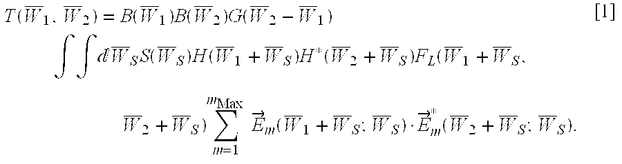
[0027] The present invention provides an improved method for modeling or simulating patterned images to be produced by lithography systems using excimer and other polychromatic lasers. The invention simulates the image by accounting for spectral line width of the polychromatic laser, the finite thickness of photoresist and other focus blurring mechanisms. As a result of the method of the present invention, OPC may be efficiently carried out under simulated polychromatic imaging.

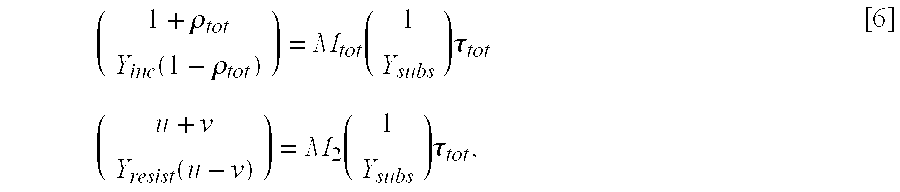
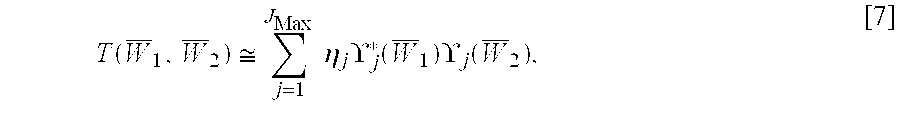
[0028] An important step in the method of the present invention is the calculation and tabulation of quantities that are referred to as polychromatic 2D imaging kernels. A kernel describes the fixed characteristics of a system which has varying inputs, where the system behavior can be described as an integral involving the input multiplied by the kernel. One version of the prior art monochromatic SOCS method is based on diagonalizing the so-called TCC matrix. In the case of polychromatic imaging, the TCCs c...


PUM

PropertyMeasurementUnit
corner anglesaaaaaaaaaa
spatial frequencyaaaaaaaaaa
dimensionsaaaaaaaaaa

Abstract

A method for determining an image of a patterned object formed by a polychromatic lithographic projection system having a laser radiation source of a finite spectral bandwidth and a lens for imaging the patterned object to an image plane within a resist layer. The method comprises providing patterns for the object, a spectrum of the radiation source to be used in the lithographic projection system, an intensity and polarization distribution of the radiation source, and a lens impulse response in the spatial domain or in the spatial frequency domain of the image. The method then includes forming a polychromatic 4D bilinear vector kernel comprising a partially coherent polychromatic joint response between pairs of points in the spatial domain or in the spatial frequency domain, determining the dominant polychromatic 2D kernels of the polychromatic 4D bilinear vector kernel, and determining the image of the patterned object from convolutions of the object patterns with the dominant polychromatic 2D kernels.

Description

BACKGROUND OF THE INVENTION [0001] 1. Field of the Invention [0002] The present invention relates generally to lithographic production of microelectronic circuits or other features and, more particularly, to a method for simulating an image of a patterned object formed in a polychromatic lithographic projection system. [0003] 2. Description of Related Art [0004] Simulation of lithography of microelectronic circuits and other features is increasing in importance as modern exposure and metrology tools increase in cost, and integrated circuit (IC) feature sizes drop well below the wavelength of light. The accurate simulation of lithographic processes can be used to eliminate many experiments, and there is huge cost incentive to do this whenever possible. Sub-100 nm features represent a significant challenge in the manufacture of ICs since such feature sizes approach the resolution limits of the lithographic imaging tools employed in IC fabrication. The practical difficulty as feature s...

Claims


Application Information

Patent Timeline
Patent Type & Authority Applications(United States)
IPC IPC(8): G03C5/00
CPCG03F1/144G03F7/70575G03F7/70441G03F1/36G03F1/70
Inventor BRUNNER, TIMOTHY A.GALLATIN, GREGG M.GORDON, RONALD L.LAI, KAFAIROSENBLUTH, ALAN E.SEONG, NAKGEUON
Owner GLOBALFOUNDRIES INC
Why Eureka
Try Eureka