Nonvolatile semiconductor storage device and method for manufacturing the same

a semiconductor storage device and non-volatile technology, applied in semiconductor devices, solid-state devices, instruments, etc., can solve the problems of difficult to obtain high integration, drive capability as a circuit may be degraded, and the tft of a complete depletion layer type cannot be formed, etc., to achieve high efficiency, prevent the increase of the contact resistance value, and low voltage

Inactive Publication Date: 2007-10-04
SEMICON ENERGY LAB CO LTD
View PDF37 Cites 61 Cited by
  • Summary
  • Abstract
  • Description
  • Claims
  • Application Information

AI Technical Summary

Benefits of technology

[0009]There is a method in which etching time for opening by dry etching is reduced by making the interlayer film thin so that etching of the semiconductor layer is suppressed. However, in a case where the interlayer film is made to be thin, parasitic capacitance of a wiring of an upper layer and a gate electrode is increased, and accordingly, drive capability as a circuit may be degraded.
[0021]Since the conductive layer provided between the source or drain region and the source or drain wiring is formed using a control gate electrode material, a nonvolatile semiconductor storage device having superior characteristics can be manufactured without losing productivity. Since the conductive layer can be manufactured by the same step as that of the control gate electrode, a nonvolatile semiconductor storage device that is capable of writing with high efficiency at a low voltage and has a favorable electric charge-holding characteristic can be manufactured without forcing manufacturing facilities to a burden.

Problems solved by technology

In the conventional nonvolatile semiconductor device as shown in FIG. 29, in a case where a thickness of the semiconductor layer is thin and a selection ratio of the interlayer film 13 to the semiconductor layer is insufficient, there is a problem in that the semiconductor layer is etched as well as the interlayer film 13 when contact holes are opened by dry etching, and accordingly a contact resistance value is increased.
When the thickness of the semiconductor layer is made to be thick in a case of using a SOI substrate, there is a problem in that a parasitic transistor between the source region and the drain region cannot be suppressed, and accordingly, a TFT of a complete depletion layer type cannot be formed.
However, in a case of wet etching, a contact hole having a high aspect ratio cannot be formed, and accordingly, high integration is difficult to be obtained.
However, in a case where the interlayer film is made to be thin, parasitic capacitance of a wiring of an upper layer and a gate electrode is increased, and accordingly, drive capability as a circuit may be degraded.

Method used


Image

  • Nonvolatile semiconductor storage device and method for manufacturing the same
  • Nonvolatile semiconductor storage device and method for manufacturing the same
  • Nonvolatile semiconductor storage device and method for manufacturing the same

Examples


embodiment mode 1

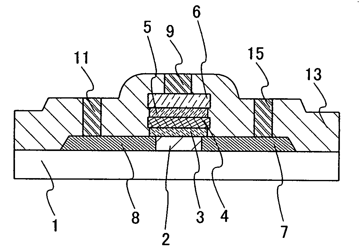
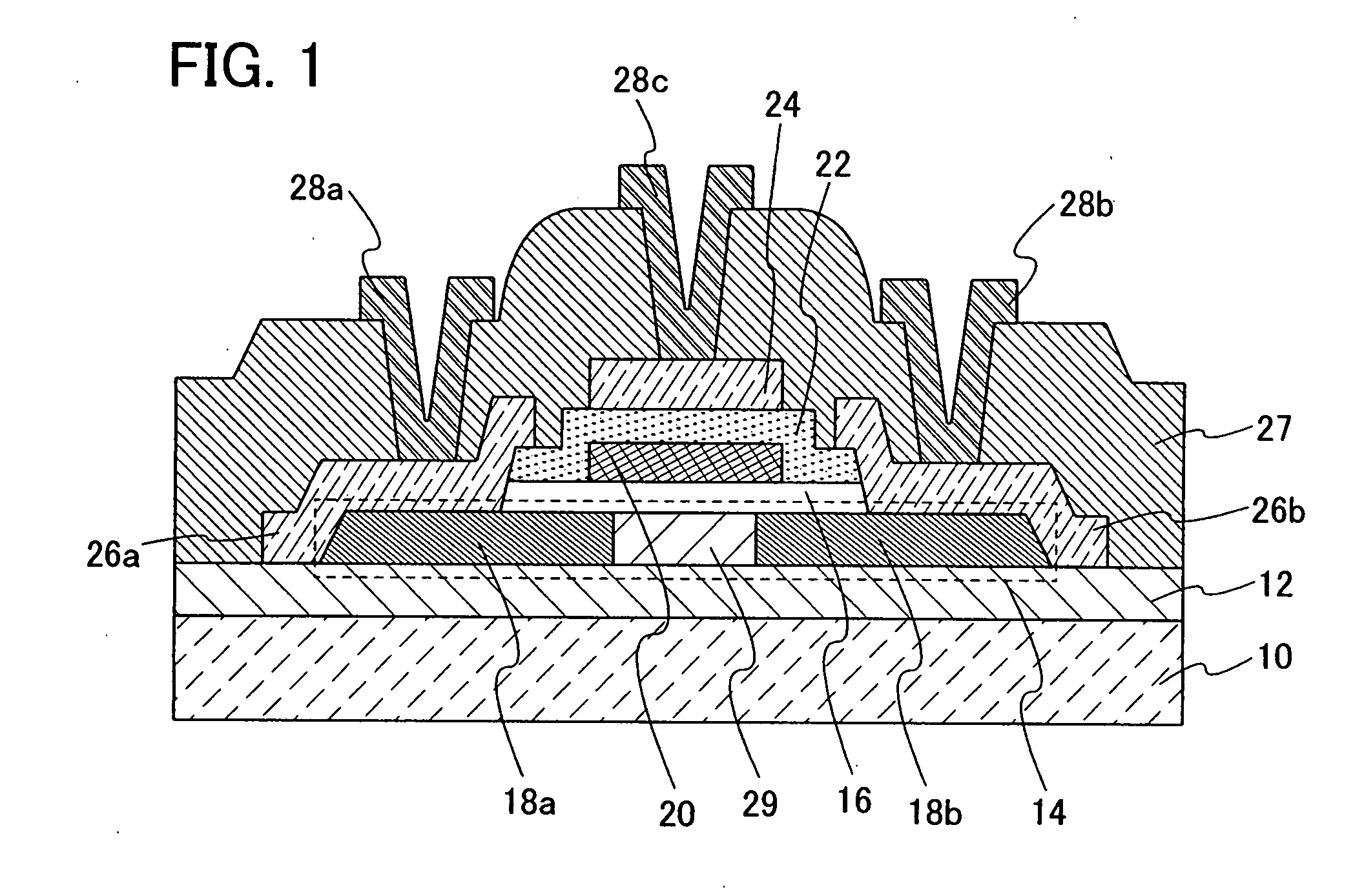
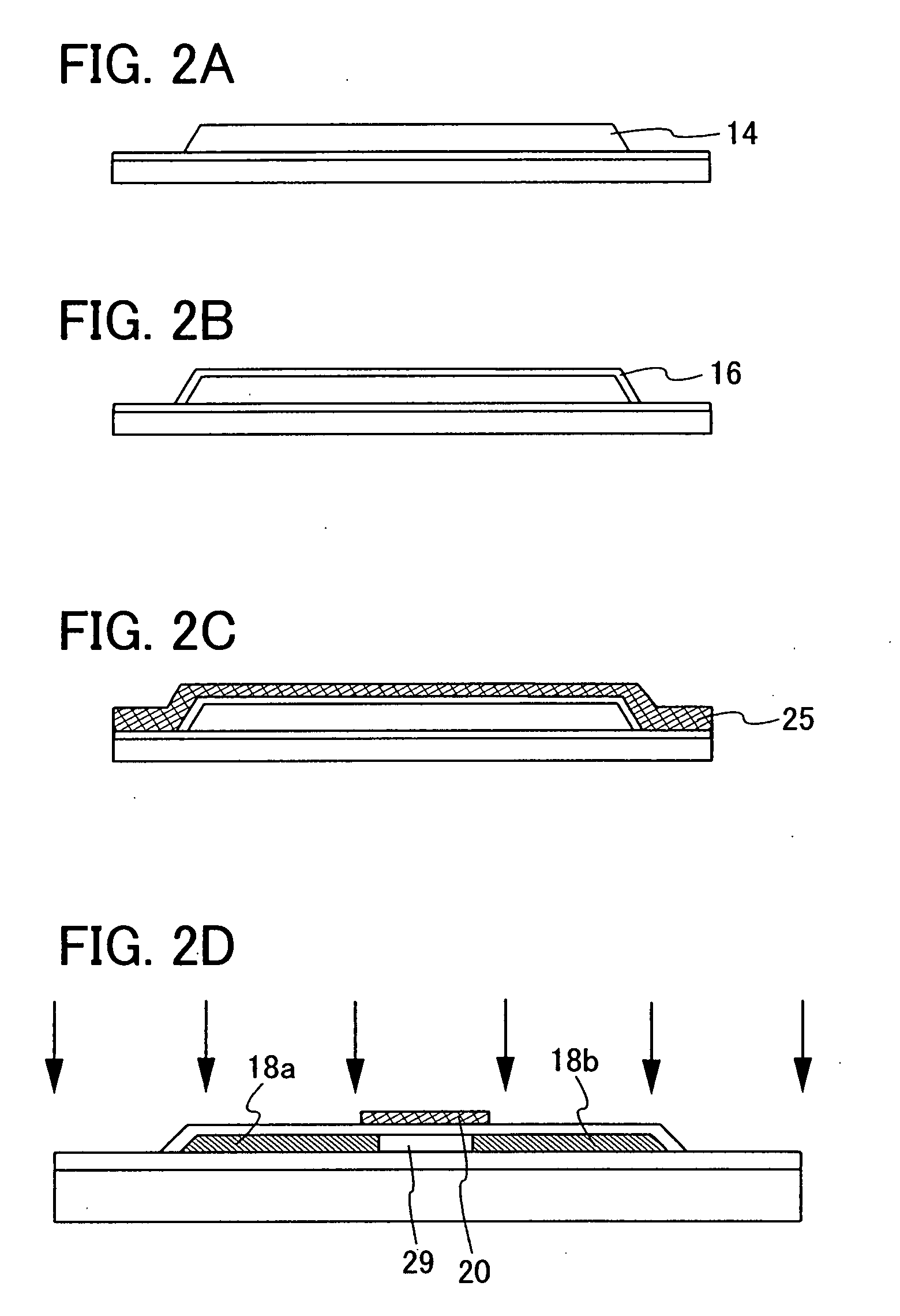
[0052]FIG. 1 is a cross-sectional view for explaining a main structure of a nonvolatile semiconductor storage device relating to the present invention. FIG. 1 particularly shows a main part of a nonvolatile memory element.

[0053]In FIG. 1, reference numeral 10 denotes a substrate; 12, a base insulating film; 14, a semiconductor layer; 29, a channel formation region; 18a and 18b, source or drain regions; 16, a first insulating film (also referred to as a tunnel insulating film); 20, a floating gate electrode; 22, a second insulating film (also referred to as a control insulating film); 24, a control gate electrode; 26a and 26b, conductive layers; 28a and 28b, source or drain electrodes electrically connected to the source region or drain regions 18a and 18b through the conductive layers 26a and 26b; 28c, a gate wiring electrically connected to the control gate electrode; and 27, an insulating film for passivation.

[0054]In the structure shown in FIG. 1, the base insulating film 12 is f...

embodiment mode 2

[0106]In this embodiment mode, a manufacturing method of a nonvolatile memory element that has a different structure from that of the nonvolatile memory element shown in FIG. 1 will be explained. In this embodiment mode, a nonvolatile memory element shown in FIG. 11 will be explained. In the nonvolatile memory element shown in FIG. 11, a control gate electrode 24 is provided with sidewalls 300.

[0107]In FIG. 11, reference numeral 10 denotes a substrate; 12, a base insulating film; 14, semiconductor layer; 29, a channel formation region; 18a and 18b, source or drain regions; 16, a first insulating film (also referred to as a tunnel insulating film); 20, a floating gate electrode; 22, a second insulating film (also referred to as a control insulating film); 24, a control gate electrode; 300, a sidewall; 26a and 26b, conductive layers; 28a and 28b, source or drain electrodes electrically connected to the source or drain regions 18a and 18b through the conductive layers 26a and 26b; 28c,...

embodiment mode 3

[0121]In this embodiment mode, a structure of a nonvolatile memory, which is different from the structures shown in FIG. 1 and FIG. 11, will be explained with reference to FIGS. 14A and 14B, FIGS. 15A to 15D, and FIGS. 16A and 16B.

[0122]In a nonvolatile memory element shown in FIG. 14A, first impurity regions (source or drain regions) 306a and 306b, second impurity regions 307a and 307b, and the like are provided in a semiconductor layer 14, and a floating gate electrode 20 is formed of a first floating gate electrode 20a and a second floating gate electrode 20b, which are different points from the structures shown in FIG. 1 and FIG. 11.

[0123]In a structure shown in FIG. 14A, a base insulating film 12 is formed over a substrate 10, and the semiconductor layer 14 having the first impurity regions 306a and 306b, the second impurity regions 307a and 307b, and a channel formation region 29 is formed over the base insulating film 12. A first insulating film 16 and conductive layers 26a a...


PUM


Abstract

It is an object to provide a nonvolatile semiconductor storage device that prevents increase in a contact resistance value due to etching of a semiconductor layer when etching an interlayer insulating film and that has superiority in a writing characteristic and an electric charge-holding characteristic, and a manufacturing method thereof. A conductive layer is provided between a source or drain region and a source or drain wiring. The conductive layer is made of the same conductive layer that forms a control gate electrode. An insulating film is provided so as to cover the conductive layer, and the insulating film has a contact hole for exposing part of the conductive layer. The source or drain wiring is formed so that the contact hole is filled.

Description

BACKGROUND OF THE INVENTION[0001]1. Field of the Invention[0002]The present invention relates to a nonvolatile semiconductor storage device that is electrically capable of writing, reading, and erasing and a manufacturing method thereof.[0003]2. Description of the Related Art[0004]A market has been expanded for nonvolatile memories, in which data can be electrically rewritten and data can be stored even after the power is turned off. There is a feature in that a nonvolatile memory has a similar structure to that of a MOSFET (Metal Oxide Semiconductor Field effect transistor) and a region capable of accumulating electric charges for a long period of time is provided over a channel formation region. An electric charge accumulating region of the nonvolatile memory is also referred to as a floating gate because it is formed over an insulating layer and insulated with circumference. A control gate is provided over the floating gate through an insulating layer (for example, Patent Documen...

Claims


Application Information

Patent Timeline
Patent Type & Authority Applications(United States)
IPC IPC(8): H01L29/788
CPCG11C16/0483H01L21/84H01L27/115H01L27/12H01L2924/0002H01L29/7881H01L2924/00H10B69/00H10B41/30
Inventor ASAMI, YOSHINOBU
Owner SEMICON ENERGY LAB CO LTD
Why Eureka
Try Eureka