

Method for manufacturing a layer arrangement and layer arrangement
a manufacturing method and technology of layer arrangement, applied in the direction of semiconductor devices, semiconductor/solid-state device details, electrical devices, etc., can solve the problems of undesirable crosstalk, high power loss, and high signal propagation time, and achieve low rc switching delay and favorable dielectric properties.
- Summary
- Abstract
- Description
- Claims
- Application Information
AI Technical Summary
Benefits of technology
Problems solved by technology
Method used
Image

Examples
Embodiment Construction
[0080] Identical or similar components in different figures are provided with identical reference numerals.
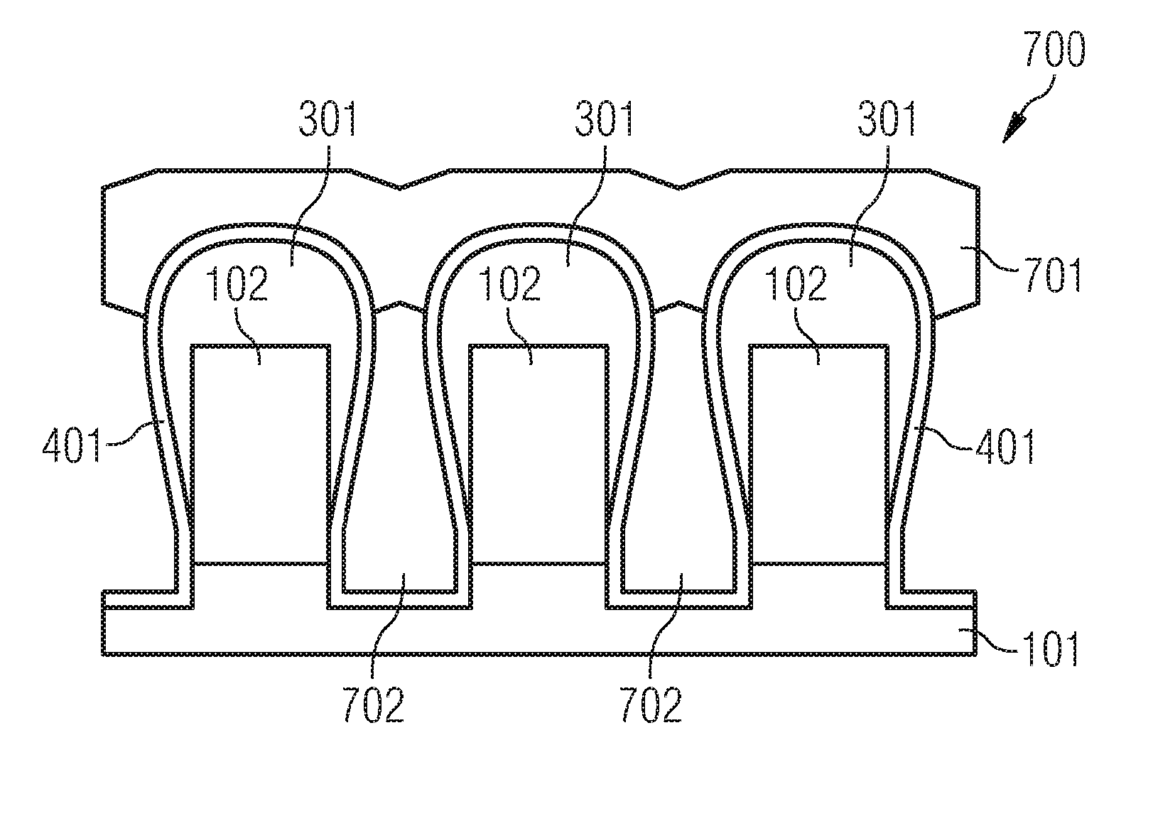
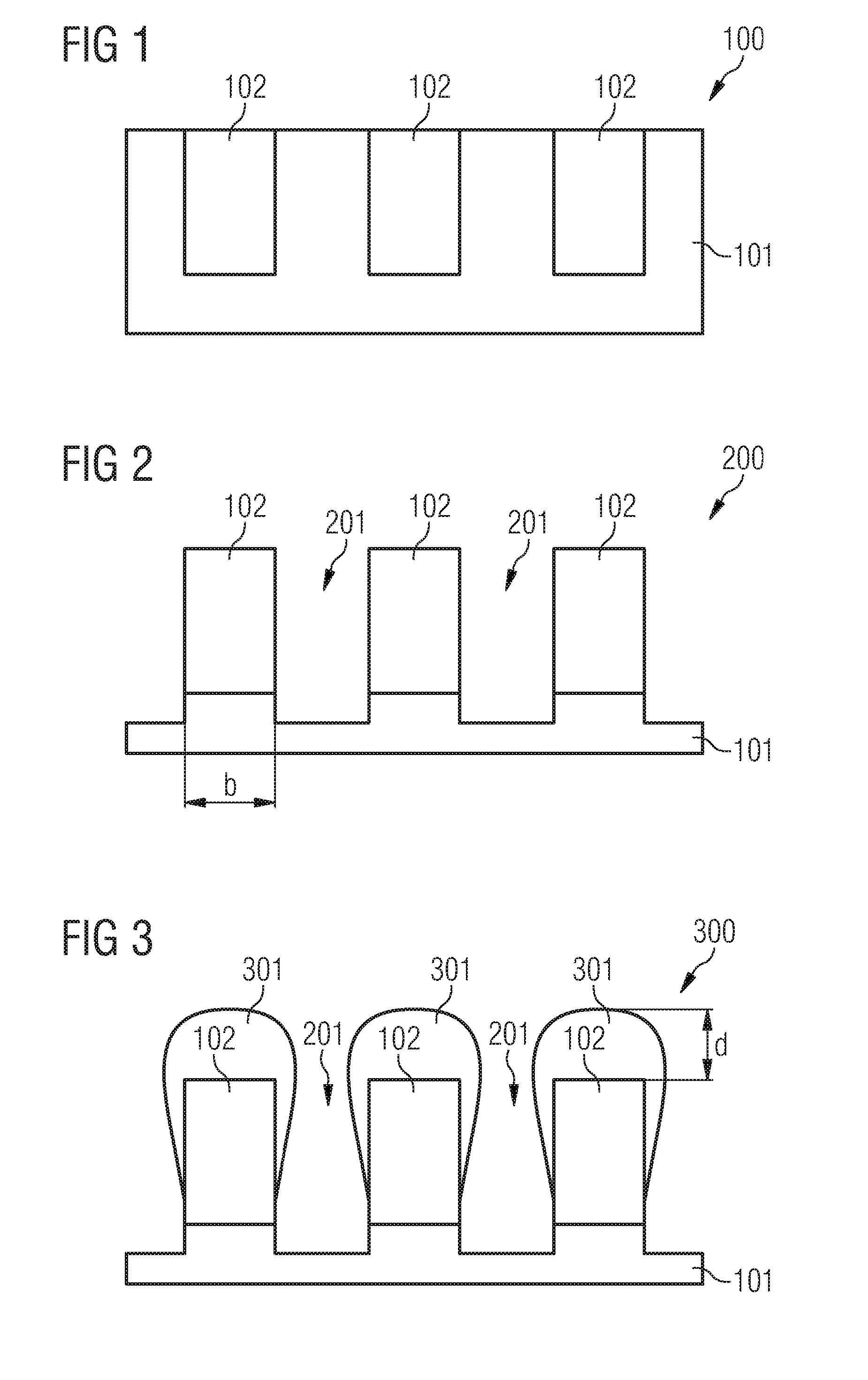
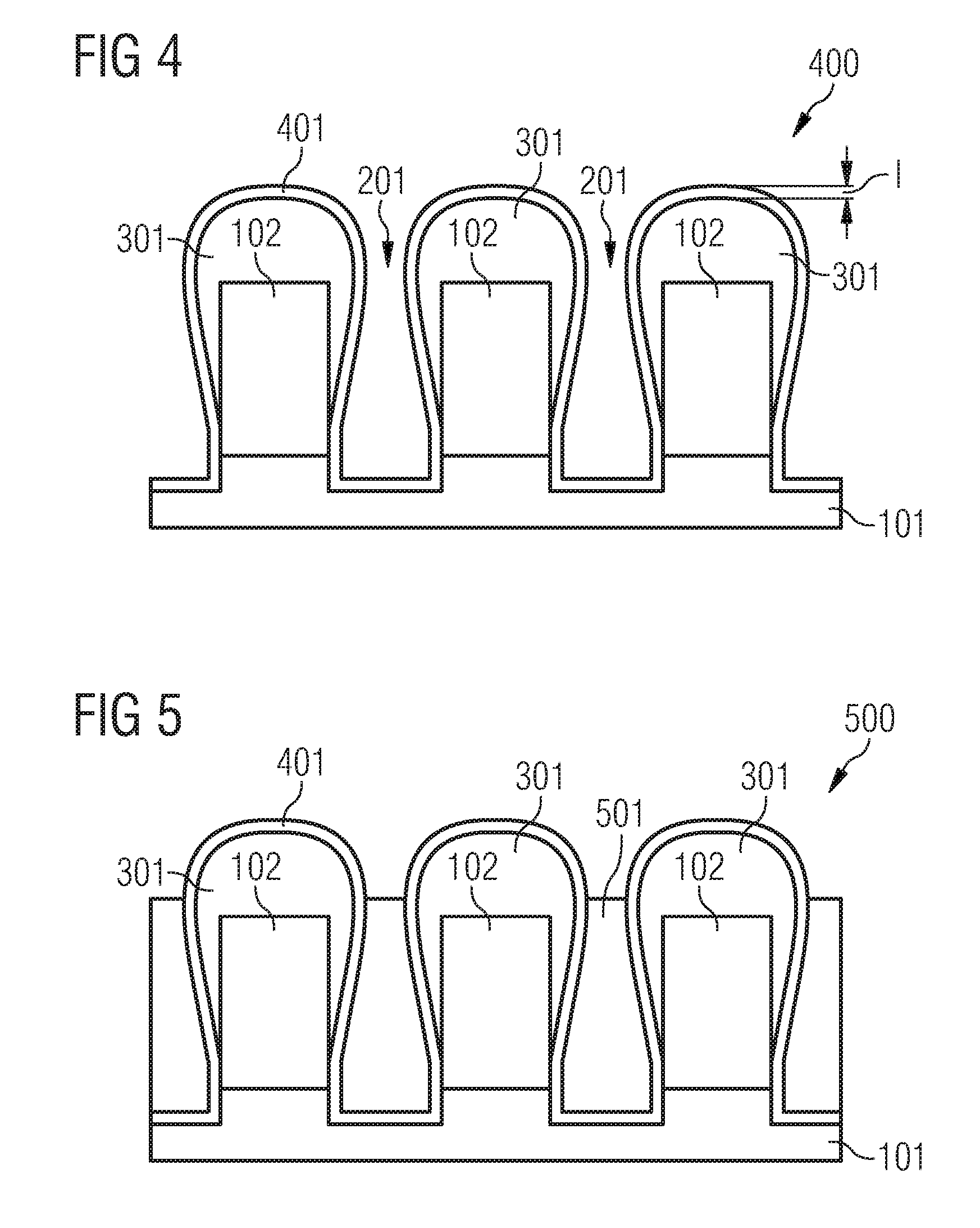
[0081] A description is given below, referring to FIG. 1 to FIG. 7, of a method for producing a layer arrangement in accordance with a first exemplary embodiment of the invention.
[0082] In order to obtain the layer sequence 100 shown in FIG. 1, trenches are formed on a dielectric substrate 101 (for example composed of silicon oxide material) using a lithography method and an etching method. Copper material is deposited on the layer sequence thus obtained. Material of the deposited copper layer is etched back using a CMP method (“chemical mechanical polishing”), whereby copper interconnects 102 are formed in the trenches. The copper interconnects 102 are therefore produced according to the damascene principle. A diffusion barrier (for example composed of TaN / Ta) not shown in FIG. 1 may be formed between a respective copper interconnect 102 and the substrate 101. A barrier laye...
PUM
 Abstract
Description
Claims
Application Information