Optical device and optical module

a technology of optical modules and optical devices, applied in semiconductor devices, lasers, semiconductor lasers, etc., can solve the problems of insufficient capacitance reduction, restricted wiring direction, and insufficient disconnection of wiring, so as to reduce parasitic capacitance, reduce capacitance, and high resistance re-growth

Inactive Publication Date: 2007-10-25
OPNEXT JAPAN INC
View PDF6 Cites 9 Cited by
  • Summary
  • Abstract
  • Description
  • Claims
  • Application Information

AI Technical Summary

Benefits of technology

[0006] With respect to a surface emitting type light emitting device and a surface illuminated type light receiving device each having a mesa portion, a high resistance re-grown layer is provided around the mesa portion. In this way, the mesa portion having a plane direction that appears in etching of a circular main structure is coated with the re-grown layer. Thus, it is possible to reduce capacitance in this portion. Further the direction of wiring is not restricted. The thickness of the re-grown layer can be set to be equal to the thickness of the main structural part. Thus, particularly, when a conductive substrate is used, a substantial reduction effect of parasitic capacitance can be expected from a combination with plural dielectric films.

Problems solved by technology

However, in the structure described in JP-A No. 5600 / 2005 or in JP-A No. 112595 / 1994, disconnection of wiring may not be fully avoided when a mesa structure is high and a dielectric film is thick.
Further, the direction of wiring is restricted in the above described structure.
Still further, the reduction of capacitance is insufficient in the above described structures.

Method used


Image

  • Optical device and optical module
  • Optical device and optical module
  • Optical device and optical module

Examples


embodiment 1

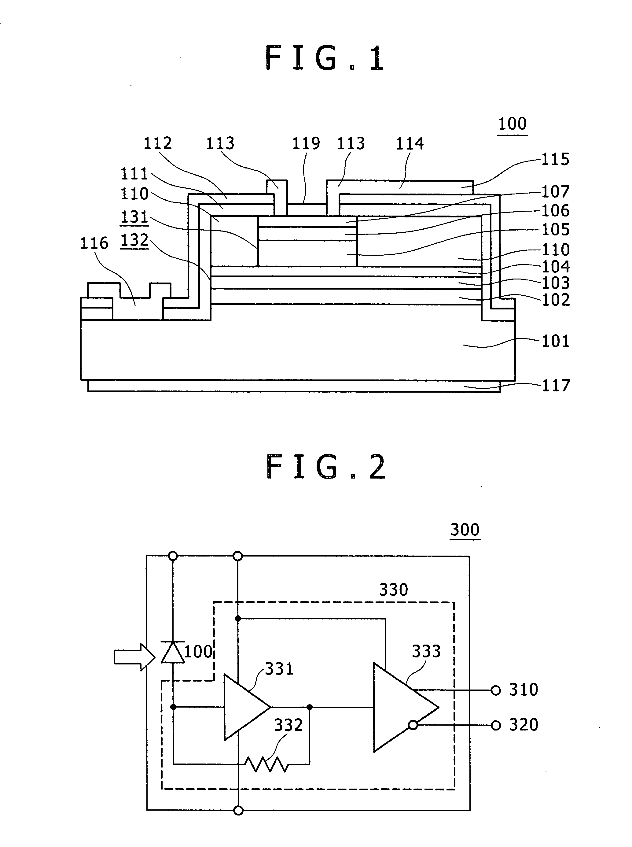
[0023] Embodiment 1 will be described with reference to FIGS. 1 and 2. Here FIG. 1 is a cross-sectional view of a top-illuminated-type APD (Avalanche Photo Diode) device. FIG. 2 is a block diagram of an optical receiver module in which the APD device is mounted. In order to avoid complexity of illustration, hatching indicating cross sections is omitted in FIG. 1 and subsequent cross-sectional views.

[0024] In FIG. 1, an APD device 100 has a structure in which a lower buffer layer 102 (conductive type: n-type InAlAs layer, impurity concentration: 1E18 cmˆ−3 (1×1018 cm−3), thickness: 0.5 μm (micrometers)), a multiplication layer 103 (n-type InAlAs layer, 1E14 cmˆ−3, 0.4 μm), a field-control layer 104 (p-type InAlAs layer, 8E17 cmˆ−3, 0.04 μm), an absorption layer 105 (p-type InGaAs layer, 1E15 cmˆ−3, 1.8 μm), a cap layer 106 (upper buffer layer) (p-type InAlAs layer, 1E18 cmˆ−3, 0.7 μm), and a p-type contact layer 107 (p-type InGaAs layer, 5E18 cmˆ−3, 0.1 μm) are laminated over an InP...

embodiment 2

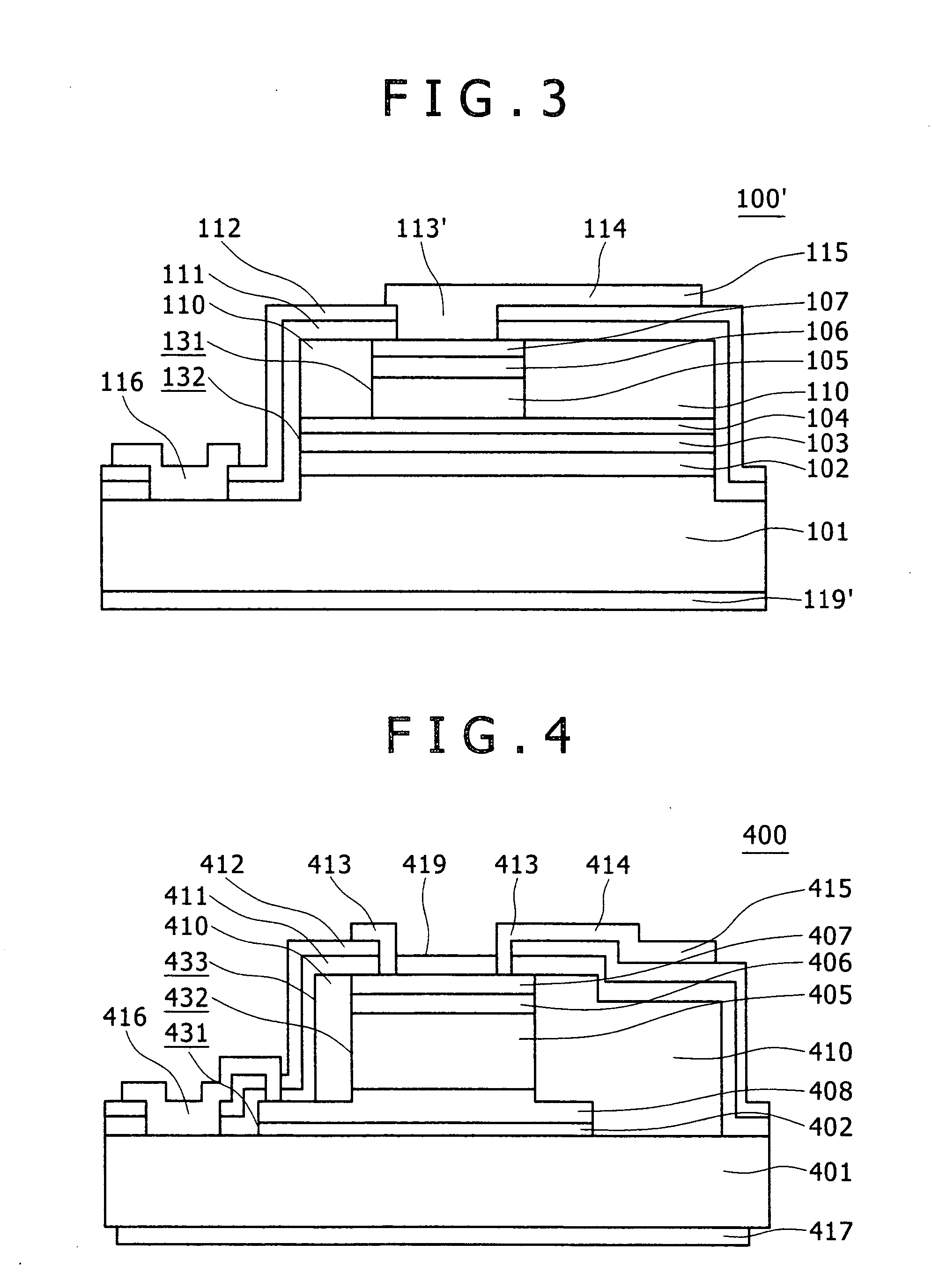
[0034] In Embodiment 1, the top-illuminated-type APD device has been described. In Embodiment 2, a bottom-illuminated-type APD device will be described with reference to FIG. 3. Here FIG. 3 is a cross-sectional view of a bottom-illuminated-type APD device. Incidentally, as the structure of Embodiment 2 is generally the same as that of Embodiment 1, substantially like parts are denoted by like reference numerals and the description will not be repeated.

[0035] In a bottom-illuminated-type APD device 100′ shown in FIG. 3, the anti-reflection coating 119 (SiN film), which is provided in the light receiving portion of the top-illuminated-type APD device in FIG. 1, is eliminated by etching and a p-type ohmic electrode 113′ is formed over the entire portion. As it is the bottom illuminated type, an anti-reflection coating 119′ is provided in place of the bottom metal film 117 for die bonding.

[0036] With the bottom-illuminated-type APD device according to the embodiment, the same effect a...

embodiment 3

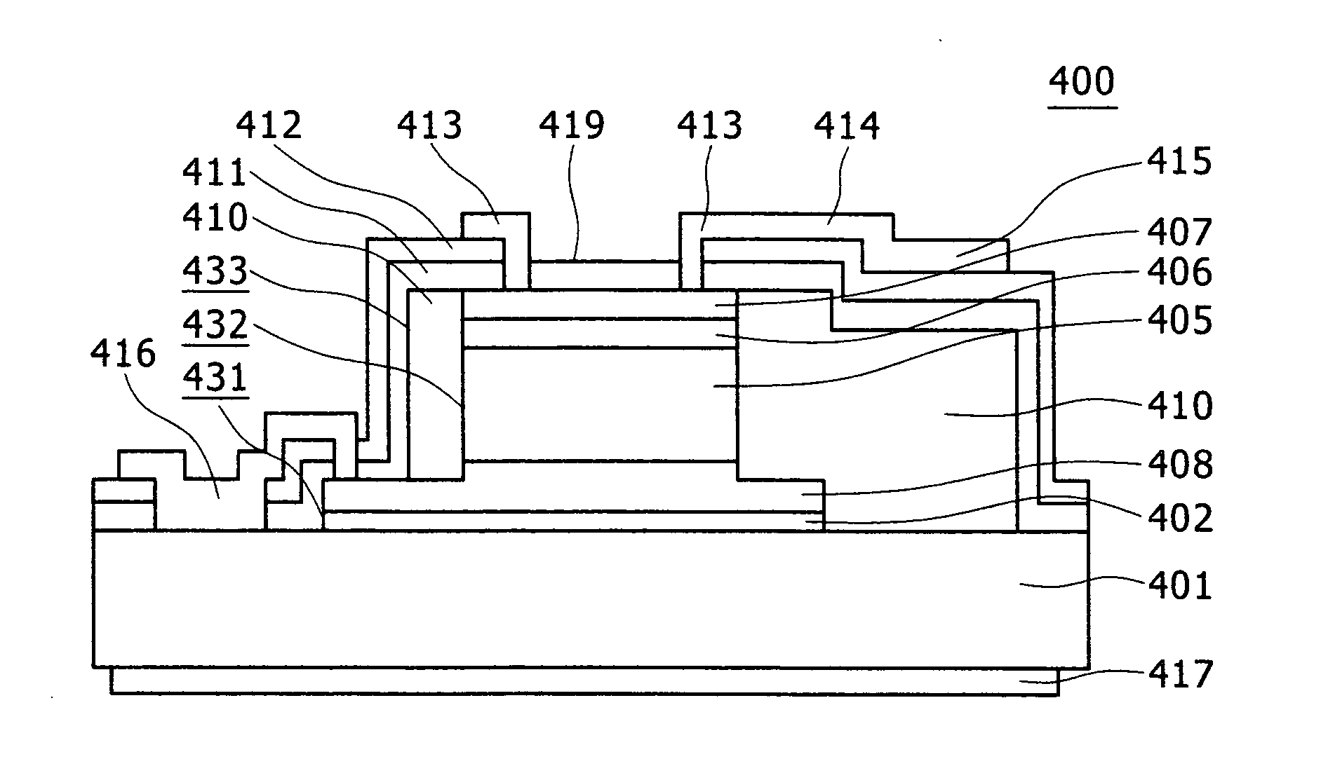
[0037] Embodiment 3 will be described below with reference to FIGS. 4 and 5. Here FIG. 4 is a cross-sectional view of a top-illuminated-type pin-PD device. FIG. 5 is a block diagram of an optical receiver module in which the pin-PD device is mounted.

[0038] In FIG. 4, a pin-PD device 400 has a structure in which a buffer layer 402 (undoped InP layer, 0.2 μm), an n-type contact layer 408 (n-type InGaAsP layer, 8E18 cmˆ−3, 0.4 μm), an absorption layer 405 (n-type InGaAs layer, 5E14 cmˆ−3, 2.0 μm), a cap layer 406 (p-type InGaAsP layer, 1E18 cmˆ−3, 0.2 μm), and a p-type contact layer 407 (p-type InGaAs layer, 1E19 cmˆ−3, 0.1 μm) are laminated over an InP (semi-insulating) substrate 401. The main active region of the pin-PD structure in the PD device 400 is formed by a three-step mesa technology. An outermost first mesa 431 is a step between the n-type contact layer 408 and the InP substrate 401. The first mesa 431 is formed by a combination of a vertical portion etched from the p-type ...


PUM


Abstract

A high resistance re-grown layer is disposed around an optical device having a mesa structure. Thus, a mesa portion having a plane direction that appears in etching of a circular main structure is coated with the re-grown layer. Because of this coating, it is possible to reduce the capacitance in this portion as well as to avoid the risk of disconnection with respect to all the wiring directions. The thickness of the re-grown layer can be set to be equal to the thickness of the main structural part. Particularly, when a conductive substrate is used, a substantial reduction effect of parasitic capacitance can be expected from a combination with plural dielectric films.

Description

CLAIM OF PRIORITY [0001] The present application claims priority from Japanese patent application serial no. 2006-116473, filed on Apr. 20, 2006, the content of which is hereby incorporated by reference into this application. BACKGROUND OF THE INVENTION [0002] The present invention relates to a semiconductor optical device, and particularly to an optical device and an optical module that are appropriate for use in optical communications. [0003] In an optical functional device (optical device) such as a light emitting device for transmitting an optical signal in direction perpendicular to a substrate or a light receiving device for receiving an optical signal from direction perpendicular to the substrate, when the optical device has a mesa-shaped active region, it is necessary to consider avoiding disconnection of wiring in a step portion and to consider reducing parasitic capacitance caused by the wiring and electrode pad. [0004] Thus, in JP-A No. 5600 / 2005, a step difference is red...

Claims


Application Information

Patent Timeline
Patent Type & Authority Applications(United States)
IPC IPC(8): H01L33/00H01L21/338H01L33/06H01L33/10H01L33/14H01L33/30H01L33/36H01L33/44H01L33/62
CPCB82Y20/00H01L31/03046H01L31/105H01L31/107H01S5/02276H01S5/0421Y02E10/544H01S5/18308H01S5/18369H01S5/3095H01S5/34306H01S2301/176H01S5/0425H01S5/04252H01S5/04256H01S5/04257H01S5/02345
Inventor KAMIYAMA, HIROYUKITOYONAKA, TAKASHI
Owner OPNEXT JAPAN INC
Why Eureka
Try Eureka